
This article discusses the basics of a step-down (buck) DC Switched-Mode Power Supply (SMPS). It should serve at an entry-level tutorial and a building step towards the more advanced designs.
Basic SMPS Topology
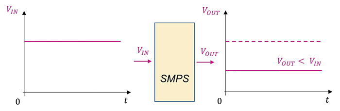
The main functional objective of the buck SMPS is to step down a DC signal, VIN, to a lower DC value, VOUT, as shown in Figure 1.
The first step in this process consists of creating a Pulse-Width Modulated (PWM) version of the DC input signal, as shown in Figure 2.
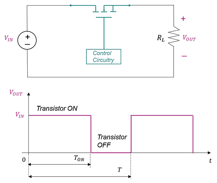
The output signal shown in Figure 2 is far from the desired output signal described in our objective. Namely: 1) it is a constant signal only when the transistor is ON, 2) its level, when the transistor is ON, is not lower than the input signal, and 3) it contains high harmonic content during the transition times, [1].
Let’s address the third aspect by placing a low-pass LC filter on the output side of the circuit, as shown in Figure 3.
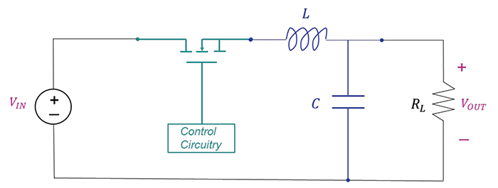
To reduce the unwanted power dissipation in the circuit, RC and RL filters are avoided, and the basic designs utilize a simple LC filter.
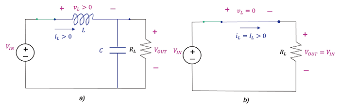
Let’s assume that the transistor is OFF, there is no energy stored in the LC filter, and the output voltage is zero. When the transistor turns ON we have the circuit shown in Figure 4(a) (assuming an ideal transistor with no voltage drop).
The output voltage gradually increases. Assuming the ON time is long enough, this voltage eventually reaches the steady-state value VOUT = VIN. In steady-state the voltage across the inductor, vL, is zero, and a dc current, IL, flows through the inductor, as shown in Figure 4(b). The magnetic energy is stored in the inductor.
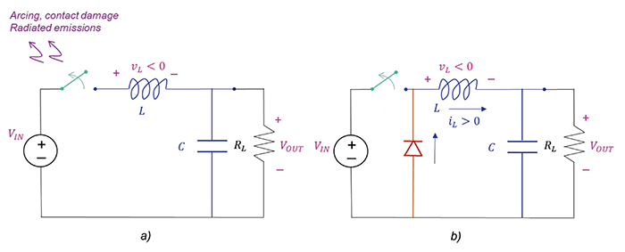
When the switch opens, a large negative voltage develops across the inductor and subsequently the switch. The magnetic energy stored in the inductor is dissipated in the arc across the switch contacts or is radiated [2], as shown in Figure 5(a).
This behavior is often destructive to the switch and some sort of a protective circuitry is required. The simplest solution is to provide a path for the inductor current during this switching event by inserting a diode in the circuit, as shown in Figure 5(b). We have arrived at one of the simplest step-down (buck) SMPS.
The basic design of this SMPS amounts to the proper choice of the components, L and C, to satisfy the imposed design requirements. The component values are determined through the circuit analysis when the transistor is ON (switch closed) and when it is OFF (switch open). The respective circuits and selected circuit variables are shown in Figure 6.
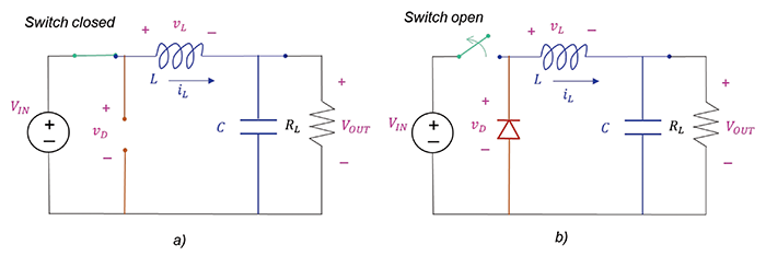
Note that in both cases, when the switch is closed and open, the inductor current is positive and flows in the same direction. If the switch remains open long enough the inductor current decays to zero and subsequently the output voltage goes to zero.
If the switch closes before the inductor current (and output voltage) goes to zero in the switching cycle, the SMPS will operate in the so-called continuous conduction mode. This is the preferred mode in EMC – it results in a smaller output ripple, smaller load-current variations, and lower EMC emissions.
When the switch subsequently opens, the output voltage rises. When it reaches the desired value, VOUT < VIN, the switch opens again. In a continuous mode and a steady-state operation, the inductor current and output voltage always stay positive and never go to zero.
SMPS Design
The following SMPS design assumes that the components are ideal – transistor and diode voltage drops are zero, inductor and capacitor are ideal (no parasitics). There are no losses in the circuitry – power supplied by the source equals the power delivered to the load. The approach discussed here is based on the material presented in [1].
The SMPS operates in a steady state, in a continuous conduction mode with the duty cycle, D, of the PWM signal equal to
![]() (1)
(1)
where the switching frequency, fSW, is constant. Switch is closed for time
![]() (2a)
(2a)
and is open for time
![]() (2b)
(2b)
When the switch is closed, the diode is reverse biased, and we have the circuit shown in Figure 7.
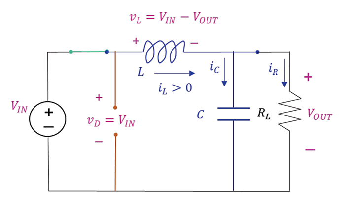
The voltage across the inductor is
![]() (3)
(3)
The voltage across the diode is equal to the input voltage, vD = VIN. From Eq. (3) we get
![]() (4)
(4)
Since this derivative is positive, the inductor current increases linearly during the time when the switch is closed. To determine the (approximate) change in the inductor current during that time we approximate the derivative in Eq. (4) by
![]() (5)
(5)
Thus, the change in the inductor current is
![]() (6)
(6)
When the switch is open, the diode is forward biased, (vD = 0), and we have the circuit shown in Figure 8.
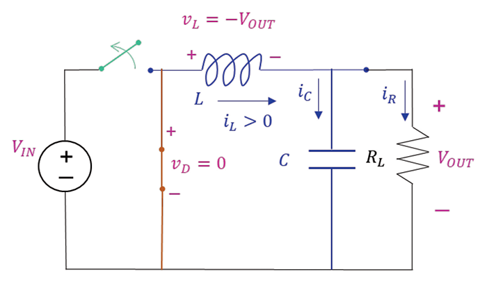
The voltage across the inductor is
![]() (7)
(7)
From Eq. (7) we get
![]() (8)
(8)
Since this derivative is negative, the inductor current decreases linearly during the time when the switch is open. The (approximate) change in the inductor current during that time is obtained from
![]() (9)
(9)
Thus, the change in the inductor current is
![]() (10)
(10)
The variations in the inductor voltage and current are shown in Figure 9.
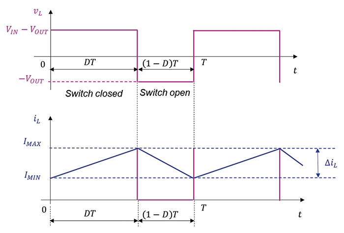
Obviously, (∆iL)closed = ∆iL)open. From Eqs. (6) and (10) we get
![]() (11)
(11)
or
![]() (12)
(12)
resulting in an input-output relationship for a buck converter
![]() (13)
(13)
Since the duty cycle is less than 1, the output voltage is lower than the input voltage. We can control the level of the output voltage by simply changing the duty cycle.
Next, let’s calculate the average, maximum, and minimum inductor currents. In a steady-state operation the average capacitor current, IC = 0, [3]. It follows that the average inductor current, IL, must be the same as the average load current, IR. That is,
![]() (14)
(14)
From Figure 9, the minimum and maximum values of the inductor current are
![]() (15a)
(15a)
![]() (15b)
(15b)
Using Eqs. (10) and (14) in Eqs. (15) we get
![]() (16a)
(16a)
![]() (16b)
(16b)
or
![]() (17a)
(17a)
![]() (17b)
(17b)
where fSW = 1/T.
Now, we can calculate the minimum value of the inductance, LMIN, for the continuous mode of operation. At the boundary between the continuous and discontinuous mode IMIN = 0. Thus, from Eq. (17a) we get
![]() (18)
(18)
or
![]() (19a)
(19a)
or utilizing Eq. (13),
![]() (19b)
(19b)
The actual value of the inductance should, of course, be larger than the minimum value given by Eqs. (19). A reasonable choice is
![]() (20)
(20)
Finally, the output voltage ripple, ∆VOUT, can be obtained by analyzing Figure 10, which shows the capacitor current and the output voltage curves, [1].

The change in the capacitor charge, ∆Q, is equal to the triangle area under the capacitor current curve when the capacitor is charging. That is,
![]() (21)
(21)
Since
![]() (22a)
(22a)
it follows that
![]() (22b)
(22b)
and
![]() (22c)
(22c)
From Eq. (10),
![]() (23)
(23)
Utilizing Eqs. (22c) and (23) in Eq. (21) we get
![]() (24)
(24)
which leads to the output voltage ripple as
![]() (25)
(25)
The relative output voltage ripple is
![]() (26)
(26)
which can be used to obtain the required capacitance in terms of the specified voltage ripple as
![]() (27)
(27)
In the design of a SMPS, the input and output voltages are usually specified. As are the load and the output voltage ripple. Once the switching frequency is chosen, the minimum inductor value can be calculated from Eq. (19b), and the capacitor value from Eq. (27).
This article presented the very basics of the simplest (and probably noisy) SMPS design. It should serve at an entry-level tutorial and a building step towards the more advanced SMPS. The next step in the design should include the non-ideal diode and transistor models, parasitics of the components and their physical limitations. To mitigate the EMC emissions, among many other considerations, an input filter [2] and a snubber circuitry [3,4] should also be implemented.
References
- Daniel W. Hart, Power Electronics, McGraw Hill, New York, NY, 2011
- Bogdan Adamczyk and Bill Spence, “SMPS Input Filter Design: Negative Resistance Approach,” In Compliance Magazine, May 2018.
- Bogdan Adamczyk and Bill Spence, “RC Snubber Design for SMPS Protection – Part I,” In Compliance Magazine, February 2019.
- Bogdan Adamczyk and Bill Spence, “RC Snubber Design for SMPS Protection – Part II,” In Compliance Magazine, March 2019.