


In my previous column — What the FAQ are CPUs, MPUs, MCUs, and GPUs? — we discussed the fact that the electronics industry is replete with acronyms, especially the three-letter variety. We also noted that we tend to learn a lot of things by osmosis, gradually (often unconsciously) assimilating nuggets of knowledge into a conceptual framework that appears to make sense… until it doesn’t.
Art Markman summed things up nicely when he said: “We see this every day in buzz words. Though we often use these words, their meanings are usually unclear. They mask gaps in our knowledge, serving as placeholders that gloss concepts we don’t fully understand.”
Analog, Digital, Mixed-Signal, and RF ASICs
Take the term ASIC, for example. What comes into your mind when you hear or see this word? If your knee-jerk reaction is to say that ASIC refers to a custom-made digital integrated circuit containing hundreds of thousands, millions, or billions of transistors, then this would tend to indicate that you come from a digital background.
Let’s start with the fact that ASIC stands for application-specific integrated circuit; that is, a custom device created to perform a specific task. Nowhere in this title do we see the word “digital.” It’s also worth reminding ourselves that there’s no such thing as an analog transistor or a digital transistor — there are just transistors that can be persuaded to perform their magic in the analog domain, in which signals operate over a continuous range, or the digital realm, which involves working with some number of defined levels.
In reality, it’s possible to create an analog ASIC containing transistors and other components connected in such a way that they implement an analog function such as an amplifier or a filter. Such devices typically contain a relatively small quantity of transistors (numbering in the tens, hundreds, or a few thousand), and these transistors are usually large, robust fellows whose shapes and sizes are fine-tuned to meet exacting specifications. (By “large” we mean “in the scheme of things,” as compared to transistors used to create digital integrated circuits — they are still incredibly tiny on the human scale of existence.)
It’s also possible to create a digital ASIC containing transistors and other components connected in such a way as to perform a whole bunch of digital functions. Such devices typically contain relatively large quantities of transistors (numbering in the hundreds of thousands, millions, or billions), and these transistors are usually small, feisty fellows who are gregarious to the extreme.
If only we could divide the world into analog and digital, life would be so simple, but — of course — it’s more complicated that that, because many ASICs contain a mix of analog and digital functionality and are therefore referred to as mixed-signal devices. Classic examples of this sort of component are analog-to-digital converters (ADCs) and digital-to-analog converters (DACs). In reality, even a device that you might regard as being “purely digital” may still contain some small amount of analog functionality in the form of functions like phase-lock loops (PLLs).
And, just to increase the fun and frivolity, it’s also possible to make radio frequency (RF) ASICs, which are known by some as radio-frequency integrated circuits (RFICs).
ASICs vs. ASSPs
Generally speaking, an application-specific integrated circuit (ASIC) is a component that is designed and/or used by a single company in a specific system. By comparison, an application-specific standard part (ASSP) is a more general-purpose device that is intended for use by multiple system design houses in multiple systems (say a USB interface chip, for example). This leads us to an interesting question — do we regard ASICs and ASSPs as falling “under” the analog, digital, mixed-signal, and RF “umbrellas” (Figure 1a), or do we visualize things as being the other way around (Figure 1b)?
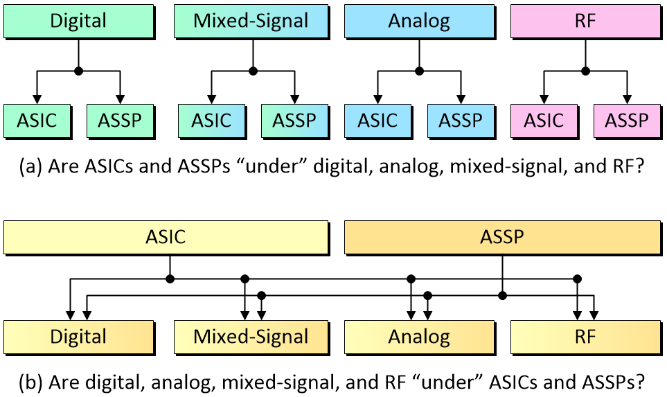
Figure 1. How do ASIC and ASSP devices relate to the analog, digital, mixed-signal, and RD domains? (Image source: Max Maxfield)
In reality (I have to stop saying that), these terms are all just “boxes” that we’ve created for ourselves, but it’s still interesting to reflect on the fact that different people think about these things in different ways. (It would be great if you would care to share which of these representations you prefer in the comments below.)
Each implementation domain (analog, digital, etc.) is typically based on its own specialized semiconductor substrates and processes, and each group of developers typically use their own specialized design, verification, and analysis tools.
For the sake of these discussions, let’s assume that we are talking about digital ASICs and ASSPs. The key point to understand here is that these devices are developed using the same design, verification, and analysis tools, and they are implemented using the same semiconductor processes and technologies.
The only thing that differentiates an ASIC from an ASSP is its intended audience and deployment — a single company in a specific system (or family of systems) versus multiple companies in a variety of systems. We might go so far as to say that a device that is considered to be an ASIC in the morning could be transmogrified into an ASSP in the afternoon if its owners simply decided to share it with the world.
One final point before we move on is that there are different types of digital ASIC (or ASSP). In terms of increasing complexity, these would be classed as Gate Arrays, Structured ASICs, Standard Cell, and Full-Custom.
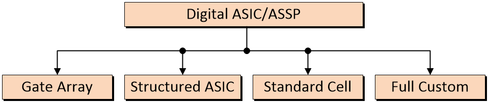
Figure 2. Different flavors of digital ASICs/ASSPs (Image source: Max Maxfield)
You will be happy to discover that we won’t delve deeper into this mire here. Suffice it to say that if you want to learn more about these little rascals, they are discussed in excruciating detail in my book Bebop to the Boolean Boogie (the first, and only, electronics book in the world to feature a recipe for seafood gumbo).
MPUs, MCUs, DSPs, FPGAs, and Memory Devices
The Bard was exhibiting his usual prescience when he had King Lear say, “O, that way madness lies.” I’m pretty sure he was contemplating what would happen if people started to try to put devices like microprocessors (MPUs), microcontrollers (MCUs), digital signal processors (DSPs), field-programmable gate arrays (FPGAs), and memory devices (DRAM, SRAM, Flash, etc.) into ASIC and ASSP “buckets.”
Unfortunately, if you’re not careful, you find yourself desperately trying to hammer a square peg into a round hole, as it were. Personally, I’ve spent far more time playing this game than was good for me. Over the years, I’ve come to the conclusion that it’s easier to say, “an MPU is just an MPU” and “an SRAM memory chip is just an SRAM memory chip,” and leave it at that.
System-on-Chip (SoC) Devices
The term System-on-Chip (SoC) refers to an ASIC or ASSP that acts as an entire subsystem. In addition to a bunch of custom functional blocks (the majority of which are typically digital, but which may include some analog and/or mixed-signal functionality), an SoC includes one or more processor cores (CPUs and/or DSPs), ancillary cores (e.g. FPUs, counters/timers), on-chip memory, and peripheral/communication cores/functions.
Some people regard SoCs as being “higher” than ASICs/ASSPs because they are based on ASIC/ASSP technologies augmented with processor cores etc. By comparison, on the basis that not all ASICs/ASSPs contain processor cores, other people think of ASIC/ASSP technologies as being the mothership, with SoCs forming a subset of these devices.
Once again, these terms are all just “boxes” that we’ve created for ourselves, but it’s still interesting to reflect that different people think about these things in different ways.
2.5D and 3D ICs
Originally, there was quite a lot of confusion about the terms 2.5D and 3D in the context of integrated circuits. A lot of this befuddlement and bemusement was caused by companies who had what we would now consider to be a 2.5D IC claiming it was a 3D IC in their marketing literature (the little scamps).
Each unpackaged integrated circuit is called a silicon die (plural die or dice). In the case of a 2.5D IC, multiple silicon dice are mounted on a base layer called a silicon interposer. The silicon interposer and its attached dice are all presented in a single package. The silicon interposer is used to connect the dice to each other and also connect to the package’s terminals (pins or pads).
In the case of a 3D IC, multiple dice are stacked on top of each other, with connections being made using through silicon vias (TSVs). A single multi-die stack could be presented in its own package, or multiple multi-die stacks could be mounted on a silicon interposer, with the entire assembly being presented in a single package.
SiPs, PiPs, PoPs, and MCMs
Multi-chip modules (MCMs) are similar in concept to 2.5D ICs, except that instead of silicon interposers, the unifying high-density interconnect (HDI) substrates upon which the dice and other components are mounted range from ceramic to printed circuit boards (PCBs).
As an aside, the individual dice that make up an MCM are known as “chiplets.” Everything is presented in a single package, which means the MCM looks like a large IC to the outside world.
MCMs come in a variety of flavors depending on the complexity of the design and the target applications and/or environments. They are typically classed as MCM-L (the substrate is a multi-layer laminated PCB), MCM-D (modules are deposited on the base substrate using thin film technology), and MCM-C (the substrate is ceramic).
The term System-in-Package (SiP) means different things to different people. Some folks think that SiP is simply a more modern and trendy name for an MCM. Others are of the opinion that a SiP falls somewhere between an MCM (because the SiP’s dice may be stacked on top of each other) and a 3D IC (because the SiP doesn’t use the highest level TSV interconnect that is the hallmark of a 3D IC).
At the end of the day, a SiP involves multiple dice and other components mounted on a common substrate — typically an HDI PCB — and presented to the outside world as a single package.
Last, but not least, for this portion of our discussions, we have Package-in-Package (PiP) and Package-on-Package (PoP). In the case of a PiP, multiple dice (each in their own chip-scale packages (CSPs)) and/or SiPs are mounted, connected, and presented to the outside world as a single package. By comparison, in the case of a PoP assembly, two or more packages are installed atop each other with an interface to route signals between them. All of these techniques allow for higher component densities in products such as mobile phones, personal digital assistants (PDAs), tablet computers, digital cameras, and… the list goes on.
COMs and SOMs
Sad to relate, the terms Computer on a Module/Computer-on-Module (COM or CoM) and System on a Module/System-on-Module (SOM or SoM) are also subject to multiple interpretations.
A very common interpretation is that of a PCB-level circuit that integrates all the functions of a system on a single module (as opposed to an SoC, which has to be mounted on a board, and which typically relies on external components such as memory devices to complete the system).
To get a better feel for this interpretation of COMs/SOMs, check out the Apalis Arm family CoMs and Colibri Arm family SoMs from Toradex. Also, check out my column COM-HPC Defines Server-Level Capabilities for Edge Computing.
An alternative interpretation is for the SOM to be no bigger than a large IC. A classic example of this interpretation is the SAMA5D27 SOM from Microchip Technology.
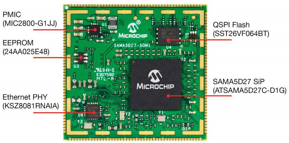
Let’s start with the SAMA5D27 SiP, which features a 32-bit ARM Cortex-A5 MCU combined with 128Mb, 512Mb, or 1Gb of DDR2 memory. This SiP can be used as a standalone device, or it can be incorporated into a larger assembly such as the SAMA5D27 SOM.
In addition to the SAMA5D27 SiP, the SAMA5D27 SOM also contains a 64Mb QSPI Flash device, a 2Kb EEPROM chip (with a pre-programmed MAC address), a 10/100 Ethernet PHY with clock, a high-performance power management IC (the MIC2800), and 103 Input/Outputs (I/Os). The result of using the SAMA5D27 SOM is to shrink the PCB size and number of layers, minimize design risk, and dramatically reduce product development time.
In Conclusion
Phew! I don’t know about you, but my mind is truly boggled. Things used to be so much simpler in the late 1970s when all we had to worry about were the dual in-line (DIL) packages associated with 7400-series devices from Texas Instruments.
Of course, if we were to try to implement something like a smartphone using the technologies of yesteryear, it would be the size of a tractor-trailer truck. The combination of today’s ASIC/ASSP/SoC technologies with SiP, PiP, PoP, MCM, CoM, and SoM packaging/deployment techniques make the high-density, high-performance systems we know and love possible.
How about you? Do you have any comments, questions, or suggestions pertaining to any of the topics we’ve discussed here?


I really am looking forward to hearing your thoughts on all of the above 🙂
Hey Max! I enjoyed your article, however, was hoping to see PMIC, Power Management Integrated Circuit. Also, DIP, Dual-Inline Package and, of course, the 300 mil wide 24 pin “Skinny DIP”.
Sir, even when we try to define & categorize things in a simple manner, they can puzzle our minds when we try to put them together (esp. mine, who was not familiar with certain things in this article). Although I was familiar (or so I believe) with certain terms like ASICs & FPGAs, I learned some new things like 2.5 D & 3D ICs.
Even though “Ignorance is bliss” can be true, but somebody has to pay the price to learn a lot and then explain things in a simple manner.
In my view, Fig 1b is better, because it can define the characteristics of a device in a more practical manner (which makes money) than a theoretical manner of Fig 1a.