

Abstract
Alloys of sulfur, selenium and tellurium, often referred to as chalcogenide semiconductors, offer a highly versatile, compositionally-controllable material platform for a variety of passive and active photonic applications. They are optically nonlinear, photoconductive materials with wide transmission windows that present various high- and low-index dielectric, low-epsilon and plasmonic properties across ultra-violet, visible and infrared frequencies, in addition to an, non-volatile, electrically/optically induced switching capability between phase states with markedly different electromagnetic properties. This roadmap collection presents an in-depth account of the critical role that chalcogenide semiconductors play within various traditional and emerging photonic technology platforms. The potential of this field going forward is demonstrated by presenting context and outlook on selected socio-economically important research streams utilizing chalcogenide semiconductors. To this end, this roadmap encompasses selected topics that range from systematic design of material properties and switching kinetics to device-level nanostructuring and integration within various photonic system architectures.
Export citation and abstract BibTeX RIS
1. Foreword
Behrad Gholipour
Nanoscale Optics Lab, Electrical and Computer Engineering Department, University of Alberta, Edmonton, Canada
Chalcogenide semiconductors, alloys of sulfur, selenium and tellurium have emerged as a critical building block for various photonic technology platforms. They are a uniquely flexible material family that can be manufactured in various forms: optical fibers, thin films, nanoparticles, monolayers and van der Waals heterostructures to name a few; and grown and patterned using complementary metal oxide semiconductor (CMOS) compatible processes. Aside from being great hosts for a variety of metallic and rare-earth dopants, they present a number of compositionally tunable properties, from photo-conduction and infrared (IR) transparency to high optical nonlinearity and persistent photorefractivity. Notably, the Lorentzian behavior of the spectral dispersion of their relative permittivity  is such that they are plasmonic and high or lowindex, at compositionally controllable wavelengths. Therefore, such materials can provide for a variety of unusual and intriguing electromagnetic wave and light–matter interaction phenomena ripe for exploration for a variety of device platforms. Utilizing this spectral dispersion, their exceptionally low refractive index and plasmonic properties in the UV–Vis part of the spectrum along with their high index low-loss dielectric properties at IR frequencies is being cultivated by a variety of researchers worldwide to support different types of static and nonlinear optical responses upon nanostructuring and hybridizing with other material systems. Additionally, they are exceptional solid electrolytes and capable of structural phase change that can be easily induced by current/illumination/electrochemistry in a reversible fashion, leading to a non-volatile, broadband change in optoelectronic properties.
This roadmap collection is divided into ten technical sections, each written from the perspective of a prominent researcher, emphasizing one theme under the umbrella of chalcogenide photonics. Each article, by bridging the history, current work and expected/needed developments, provides crucial insight into future pathways to the reader. As in any roadmap, these features and the juxtaposition between them define the bulk of the research landscape. In this way, the roadmap endeavors to position current work within the larger scientific community and provide researchers with awareness of developments and possible connections between sub-fields in order to facilitate and foster new scientific connections and engineering approaches.
Here, we present a brief overview of the ensuing sections of this roadmap, their fundamental importance and relation to other sections. We start with the need to develop a fundamental understanding of the static and dynamic optoelectronic properties of chalcogenide semiconductors at the atomic level. In this pursuit, in a section by Elliott et al, Ab-initio (AI), density functional theory (DFT)-based computer simulations of molecular dynamics (MD) that play an essential role in understanding the atomic and electronic structure of chalcogenide glasses (ChGs) during phase transformations and other optically induced metastabilities is discussed. The need for systematic material design strategies is further exemplified in a section by Müller et al where a powerful toolbox to understand, design and optimize chalcogenides for photonic applications based on recent advances in understanding the interplay between chemical bonding and crystallization kinetics is discussed, providing a useful tool for designing fast switching, high modulation contrast reconfigurable devices. Computational material design techniques are increasingly coupled with experimental high-throughput combinatorial stoichiometric engineering techniques. As discussed in a section by Hewak et al, combinatorial methods and high-throughput screening techniques have emerged as a powerful tool to accelerate material discovery and stoichiometric optimization for specific application-dependent properties across the vast compositional window at our disposal when utilizing chalcogenide semiconductors.
Controlling the static and dynamic optical properties of chalcogenide semiconductors in increasingly scaled optoelectronic device platforms is further pursued through bottom-up or top-down nanostructuring. In this realm, transition metal dichalcogenides (TMDs) which are layered, van der Waals-bonded solids with intriguing physical properties have justifiably garnered much attention recently. As discussed in a section by Li et al, TMDs feature optical transformations that can be triggered by electric fields, charge injection, electrochemical reactions and strain. Here, the availability of non-thermal switching mechanisms that take advantage of the small atomic displacements during switching in the layered crystal structure, suggest that fast, high-endurance switching may be possible through this route. In contrast, a top-down approach to layered nanostructuring at slightly larger dimensions in order to control switching energies is discussed by Simpson et al. Here, chalcogenide superlattices are utilized to confine the phase transition to a plane at interfaces in a multilayered all-chalcogenide structure. This reduction in dimensionality lowers entropic losses, reducing the energy needed to switch the state of the material.
Cui et al takes this further and discusses how subwavelength nanostructuring has also been utilized extensively in the last decade to control the static optical properties of chalcogenide semiconductors and enhance their switching dynamics by creating optically resonant media at specific wavelengths of interest from the ultra-violet to the microwave bands of the electromagnetic spectrum. Referred to as metamaterials and metasurfaces, these nanostructures enable various beam steering, modulation and focusing functionalities for incorporation into a range of photonic systems that require adaptive and dynamic control.
Chalcogenide semiconductors are also revolutionizing a range of photonic integrated systems. As detailed in a section by Eggleton et al, they have become a cornerstone of nonlinear optics as they offer ultrafast third-order nonlinearities, ideal for signal processing, where the discovery of on-chip stimulated Brillouin scattering (SBS) has opened a new frontier for microwave photonics and sensing. Further gains have been realized through the development of microstructured and step-index optical fibers using ChGs designed to engineer and tailor the dispersion properties leading to more efficient parametric processes for applications such as supercontinuum generation. In a section by Rochette et al, chalcogenide optical fibers are therefore discussed as a crucial component for lasing systems especially those operating across mid-IR wavelengths. Driven by the rise of silicon-photonics, optical systems and devices research has moved from the long-distance communication domain to intra- and inter-chip architectures. In this domain, reconfiguration of silicon photonic integrated circuits (PICs) relying on the volatile thermo-optic or electro-optic effect of silicon usually suffers from large footprint, small on/off ratios and high energy consumption. Therefore, as outlined in a section by Karnik et al, a huge global effort is underway to integrate ChGs within various silicon photonic architectures for telecommunication and emerging neuromorphic computing applications. Furthermore, aside from their phase change and nonlinear properties, ChGs also exhibit high levels of photoconductivity which find huge applications in sensing and imaging detectors as outlined in a section by Kasap et al.
Through this collection, it is clear that chalcogenide photonic devices hold the key to major breakthroughs in a variety of different technology platforms, giving rise to more efficient, smaller or lighter devices with a myriad of different applications.
On the path to commercialization, when considering economic barriers and lab to market journey for chalcogenide photonics-based products, there are a number of challenges that have traditionally had to be overcome. While the chalcogenide semiconductors present an ultrawide transmission window that depending on composition can stretch from visible to far-IR wavelengths, optical losses, especially in the visible and near-IR spectral bands due to contaminants found in the raw materials used to make ChGs, have historically hindered widescale commercial uptake in applications requiring low propagation losses. This barrier has been drastically lowered in recent years and will continue to be lowered with cleaner, more precise glassmaking, physical vapor deposition (PVD) and device nanofabrication processes that will in turn reduce the cost of such devices going forward.
Therefore, the future lies in the interconnected progress made in improving fabrication processes, systematic design and structuring of material platforms and their efficient integration within various system architectures. With the advent of the internet of things in conjunction with the increased interest in neuromorphic and quantum computing, the demand for adaptive sensing and information processing devices is increasing daily. This will be a major motivator in the coming decades that will drive the continued global interest in chalcogenide photonics.
2. Ab-initio (AI) computer simulations of phase transformations and optically-induced metastabilities in chalcogenide glasses (ChGs)
S R Elliott
Physical and Theoretical Chemistry Laboratory, University of Oxford, Oxford OX1 3QZ, United Kingdom
Status
AI, DFT-based computer simulations, especially MD, play an essential role in understanding the atomic and electronic structure, and the concomitant atomic/optoelectronic behavior, of materials, such as ChGs whose phase transformations and optically induced metastabilities permit optical and electronic non-volatile memory (NVM) and reconfigurable optical applications. MD simulations involve computing the spatial and temporal evolution of a collection of atoms in a simulation box, usually cubic and with periodic boundary conditions to eliminate surface effects, mutually interacting via an interatomic potential. Models of glassy materials are usually simulated using a 'melt-quench' protocol to emulate actual vitrification, in which an equilibrated high-temperature liquid state of the modeled material is thermally quenched to a low temperature by removal of energy. Due to computing-resource restrictions on the duration of simulation runs, this quenching procedure is usually sufficiently fast for vitrification to occur. Exceptions are very bad glass-formers, for which crystallization can readily occur; examples are phase change materials (PCM), such as germanium antimony telluride (Ge2Sb2Te5 (GST)), used in phase change random access memory (PCRAM).
Traditionally, MD simulations have been performed using 'empirical' interatomic potentials, generally having simple functional forms which greatly speed up simulations, but which are often inaccurate. However, such MD simulations can only provide atomic, and not electronic, information, since no information about electron wavefunctions is involved. Hence, nowadays ab-initio molecular dynamics (AIMD) simulations are preferred, in which electron wavefunctions are calculated quantum-mechanically during the simulation, typically making use of the DFT approximation to make the simulations tractable. If the wavefunctions are modeled as plane waves, this results in simulations scaling cubically with the system size, i.e. as O(N3), where N is the number of atoms in the simulation box. Although this typically limits model sizes to be <1000 atoms, simulation durations to be <1 ns and typically only one model is produced (rather than an ensemble), the advantage of this approach is that interatomic interactions are calculated as accurately as reasonably possible, and electronic, as well as atomic, properties can be calculated. Thus, it is advantageous to develop linear-scaling (O(N)) methods in order to study larger models. In addition, attention needs to be paid to increasing the accuracy of the interatomic potentials by improvements to the exchange-correlation functional, accurate inclusion of non-covalent (e.g. van der Waals) interactions, etc.
Current and future challenges
ChGs exhibit a wide range of optically induced photostructural and associated metastabilities, e.g. photo-darkening and photo-induced refractive-index changes, photo-crystallization etc [1]. In addition, glassy (g-) tellurides, such as GST, exhibit (∼ns) crystallization when subjected to optical or Joule-heating voltage pulses (and the reverse light/voltage-pulse-induced transformation back to the g-state, via an intermediate liquid state). Glassy and crystalline (c-) phases of GST exhibit a marked difference in optoelectronic properties: the c-state is optically reflective/electrically conductive, whereas the g-state is optically non-reflective/electrically resistive. This property contrast therefore allows the material to act as a phase change NVM, wherein binary bits of information {0,1} are written as metastable structural states of the material with readably different optoelectronic behavior [2]. Experimental investigation of the atomistic/electronic processes underlying such changes is very challenging because of the very short timescales involved (ps–fs for optical pulses, ns–ps for voltage pulses), coupled with the very small spatial dimensions involved (a few nm for PCRAM). Thus, computer simulations, e.g. DFT-based MD which can simulate atomic processes in models a few nm in size and for a few ns in duration, are essential to an understanding of the mechanisms involved.
A knowledge of the precise nature of chemical bonding in g- and c-chalcogenides is central to understanding the mechanisms responsible for their optical/voltage-pulse-induced metastabilities. The low (2–3) atomic coordination of chalcogens, such as Te, and the existence of their p-like lone-pair (LP) 'non-bonding' states, lying at the top of the valence band in the electronic density of states, and which can participate in weak van der Waals or stronger coordinate- (dative-)bond interactions, are primarily responsible for the facile photostructural changes and the ultra-rapid crystallization of GST and similar PCM materials. DFT calculations show that the bonding character in g-GST is predominantly covalent-like, but that in c-GST is mostly 'hyperbonding-like', where Te p-LPs interact with adjacent antibonding states of Ge–Te/Sb–Te bonds to form near-linear trimeric dative-bonding configurations [3, 4]. (An alternative model of the bonding in c-GST etc is that it is 'metavalent-like', i.e. part-metallic and part-covalent, with an average of one electron per bond [5, 6].) DFT calculations show that hyperbonds are much more polarizable than are normal covalent bonds, thereby accounting for the observed optoelectronic property contrast between c- and g-states of GST and other PCRAM materials [3, 4].
AIMD simulations have also shed much light on the structural transformations associated with the crystallization of PCM materials. The entire PC cycle for GST, glass–crystal–liquid–glass, was first simulated by AIMD in 2008 [7]. The role played by four-membered Ge–Te–Ge–Te rings, the characteristic structural motif of the rocksalt metastable phase of c-GST, and which are also present in the glassy state, in facilitating ultra-rapid crystal nucleation was thereby revealed [8]. In addition, the crystal growth in PCRAM materials was revealed by AIMD simulations [9] to be due to facile local, non-diffusional structural transformations between defective octahedral and other coordination polyhedra in the heated glassy/liquid state, due to the transient formation and breaking of hypervalent bonds.
Advances in science and technology to meet challenges
The most accurate computer simulations for materials involve the use of DFT, and related approximations, to calculate electronic wavefunctions, energies and interatomic forces. However, MD-simulation (and electronic-structure) codes using plane-wave representations of wavefunctions scale as O(N3). In order to circumvent this severe computer-resource limitation in constructing models containing many thousands, even millions, of atoms to study large-scale behavior, one requires methods which are O(N) in system size, but which also, ideally, have DFT levels of accuracy for calculated energies and forces. One such approach is to use local descriptions of wavefunctions instead of plane waves.
An alternative approach, obtaining O(N) interatomic potentials, has been to use 'machine-learning' (ML) techniques which, in this context, are simply sophisticated tools to obtain high-dimensional interpolated fits to potential-energy surfaces, e.g. calculated by DFT for a range of small models with representative structures. The two most common types of ML-based interatomic potentials are artificial neural-network potentials (NNPs) [10] and Gaussian approximation potentials (GAPs) [11]. The central approximation of both NNPs and GAPs is that the total energy, E, of a system can be written as a sum of local energies, i
, where each of these local atomic energies is a function of the local atomic environment of the ith atom, the latter being defined using a set of structural descriptors. ML potentials have the advantage that local atomic energies can be obtained, unlike for plane-wave methods, but the disadvantage that electronic information is not available. If the latter is required, DFT-based electronic-structure calculations for ML models of <1000 atoms in size must be carried out.
Two types of DFT-accurate ML potentials have been developed for PCRAM materials. The first are NNPs for GeTe [12, 13]. These ML potentials have been used in simulations of g-GeTe for several applications, including crystallization of the amorphous state, studies of atomic dynamics in the supercooled liquid state, thermal behavior of the amorphous state and electronic behavior ('resistance drift'). One NNP for GeTe [12] was later extended by including surface-containing configurations in the fitted database, to simulate large nanowires of GeTe.
The second ML potential is a GAP for GST [14]. Models of g-GST containing up to 24 300 atoms were simulated using this GAP potential, and glassy models of this material also were simulated with quench rates from the liquid down to as low as 1 K ps−1 [15]. Chemical transferability of the ternary GST GAP potential was successfully demonstrated [16] by using it to simulate the binary material, g-Sb2Te3, one end-member of the compositional tie line with GeTe containing the canonical PCM composition, Ge2Sb2Te5. An ensemble of 30 independent 315-atom models of g-GST were simulated by MD with the same preparation protocol and using the GST GAP potential, in order to obtain a statistical insight into the occurrence of localized electronic states lying in the band gap, as calculated by DFT methods [17].
It seems that there has been only one other ML (GAP) potential that has been developed for a glassy chalcogenide, viz. g-AsTe3 [18]. This was used to construct an MD model, along with DFT-based MD models, for an atomic-structural study.
Concluding remarks
Modeling of glassy materials, such as chalcogenides exhibiting phase transformations and optically induced metastabilities, has advanced greatly recently with the development of machine-learned, DFT-accurate, linear-scaling interatomic potentials, allowing for the construction of models containing many thousands of atoms. This allows for the study of large-scale atomic dynamics, such as phase transformations (e.g. crystallization). However, there is currently a lack of state-of-the-art calculations of electronic transitions in chalcogenides, e.g. using G–W or time-dependent methods, in order to obtain a deep understanding of the origin of optically-induced metastabilities in these materials.
Acknowledgments
The enormous contribution of Dr Tae-Hoon Lee to the electronic structure calculations and simulations of GST, of Dr Felix Mocanu to the development of the GST GAP and of Dr Konstantinos Konstantinou to its applications described herein is gratefully acknowledged.
3. Switching kinetics by design: tailoring chalcogenides for photonic applications
Maximilian J Müller and Matthias Wuttig
Institute of Physics IA, RWTH Aachen University, Aachen 52074, Germany
Status
Chalcogenides show tremendous potential for photonic applications ranging from memories to optical sensors and displays [19, 20]. To meet the demands of these applications, suitable chalcogenides have to possess an unconventional property portfolio which includes the ability to rapidly and reversibly switch the material between two different phases, often an amorphous and a crystalline state [21]. These two phases differ significantly in their optical and electronic properties for a subgroup of chalcogenides and related compounds, which are frequently described as phase change materials (PCMs). Yet optical contrast, i.e. a change of optical properties, is not the only requirement that these materials have to meet. Besides a set of crucial optical properties, which are listed in table 1, it is also important that the switching process is fast and consumes as little energy as possible [22].
Table 1. Set of requirements for a material to realize active photonic switches.
| Optical properties (for the desired wavelength of application) | Δn/Δk ≫ 1 [22] |
| k ≪ 1 [22] suitable band gap | |
| Switching kinetics | Low power/energy consumption, i.e. energy density <0.03 J μm−3 |
| Fast switching process, i.e. switching time below 10 ns |
This immediately raises the question: which materials possess the required unconventional property combination? It would be highly beneficial if one would be able to identify and tailor suitable chalcogenides for photonic applications, i.e. design their switching kinetics and optical properties. Reaching this goal requires a fundamental understanding of material properties. Optical properties, as described by the dielectric function (ω) are closely related to the electronic states in the vicinity of the Fermi level EF. Crystalline PCMs like GeTe, Sb, Sb2Te3, GeSb2Te4 and Ge2Sb2Te5 utilize an unconventional bonding configuration, which is responsible for many of their properties. The electronic states close to EF are dominated by p-electrons, which form a σ-bond with p-electrons of neighboring atoms [5, 6]. Unlike in conventional covalent bonds, where an electron pair is formed between adjacent atoms, crystalline PCMs typically form a σ-bond with adjacent atoms, which only contains half an electron pair, i.e. forms a 2c–1e bond. This should give rise to a metallic state, since the corresponding band is half-filled. However, this configuration, which has been denoted as an 'incipient metal' is unstable against the opening of a band gap, either due to a small lattice distortion, or due to moderate electron transfer between the atoms involved [5, 6]. This type of bonding differs considerably from metallic, covalent and ionic bonding and has been coined 'metavalent' bonding [23].
Current and future challenges
Interestingly, the optical properties of crystalline PCMs are closely related to the chemical bonds involved. As sketched in figure 1, the transitions which govern the optical properties of crystalline PCMs in the visible and near-IR regime are transitions between predominantly p-like states in the valence and conduction band. These states and their overlap, which strongly influences the corresponding dielectric function, as well as their band gap are controlled by the electron transfer between adjacent atoms and the size of the Peierls distortion. These two quantities can be described by quantum chemical calculations, i.e. the number of electrons transferred (ET) and the number of electrons shared (ES) between adjacent atoms [24]. We can hence design the optical properties of crystalline chalcogenides by ES and ET. This is schematically depicted in figure 1. In amorphous PCMs, the corresponding Peierls distortion is more pronounced, leading to a smaller orbital overlap and hence lower absorption. This explains the optical contrast between the two different phases.
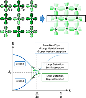
Figure 1. Illustration of the bond formation in GeTe and the resulting band structure. Atomic orbitals of Ge and Te responsible for bond formation in GeTe are depicted at the top. σ‐Bonds are formed from p-orbitals, which are occupied by about half an electron pair (ES ≈ 1), resulting in a metallic band (blue curves at the bottom of the figure). However, moderate charge transfer and/or a moderate Peierls distortions result in a small band gap. Modified after [25].
Download figure:
Standard image High-resolution imageYet, understanding how to tune optical properties is only one of the challenges that need to be surmounted to realize superior photonic switches based on chalcogenides. It is also important to tailor the switching kinetics. A major advantage of PCMs is their ability to realize non-volatile switches. Nevertheless, the stability of the different phases has to be guaranteed for the temperatures the device is exposed to. Furthermore, since crystallization is slower than amorphization, it is important to minimize the time to crystallize an amorphous chalcogenide. Until recently, suitable PCMs have been mostly identified and optimized by either intuition or extensive variations of stoichiometry. The successes in understanding the origin of optical properties and property contrast between the amorphous and crystalline state now call for systematic studies of crystallization kinetics as a function of systematic changes in chemical bonding, as described by changes of ES and ET. Furthermore, it would be highly beneficial to understand the interplay between switching kinetics and optical properties of the chalcogenide switches. Finding a similar classification scheme to describe trends for crystallization, vitrification and optical properties would drastically simplify the search for suitable materials for tailored photonic applications.
In the following we will sketch advances to reach these two goals.
Advances in science and technology to meet challenges
Utilizing an optical tester, the minimum time for crystallization τ for different PCMs has been measured [26]. Interestingly, systematic trends have been identified for the crystallization speed, which increases by more than five orders of magnitude in the region between covalent and metallic bonding, i.e. for metavalently bonded solids. Specifically, the increase of switching speed is correlated by a reduction of the number of ES between adjacent atoms. It has been demonstrated that the decrease in ES is accompanied by an increasing optical reflectance, indicative of a decreasing size of the Peierls distortion. Presumably, this leads to weaker bonds, which facilitate atomic rearrangements [26]. Figures 1 and 2 provide a tool-box for optimizing the optical contrast and increasing the switching speed. Yet, there are two challenges. The fastest switching chalcogenides are such bad glass-formers that they crystallize so rapidly at elevated temperatures, such that the amorphous state lacks stability already slightly above room temperature. Recent experiments provide a potential approach to solve this problem. This study shows that the undercooled liquid of PCMs like Ge15Sb85 and Ag4In3Sb67Te26 is characterized by a liquid–liquid phase transition, which marks the onset of Peierls distortions at lower temperatures. Presumably, this phase transition provides the fast atomic rearrangement required for fast crystallization at elevated temperatures, yet stability against recrystallization at lower temperatures [26]. Furthermore, fast switching chalcogenides often have a rather low band gap, hence limiting the range of wavelengths for which chalcogenide-based devices can be employed. Hence, it needs to be seen if metavalently bonded chalcogenides can also be utilized to realize photonic switches in the visible range. Yet, the systematic understanding developed now provides two coordinates which can be used to rapidly scan parameter space and identify potential sweet spots.

Figure 2. Change of kinetics with bond indicators. Dependence of the minimum crystallization time upon two chemical bond quantifiers, the number of ET and shared between adjacent atoms. A pronounced decrease of the minimum time to crystallize is observed in the metavalent bonding region (green background) between covalent (red) and metallic bonding. Modified after [26].
Download figure:
Standard image High-resolution imageConcluding remarks
Recent advances in understanding the interplay between chemical bonding, optical properties and crystallization kinetics provide a powerful tool-box to understand, design and optimize chalcogenides for photonic applications. It thus appears rewarding to employ the crucial chemical bond descriptors ES and ET as parameters guiding the search for systematic trends for the properties listed in table 1. These insights should help in identifying potential speed and property limits for chalcogenide-based photonics, and hence provide a useful tool-box for designers of optical systems.
Acknowledgments
This work was supported by the Deutsche Forschungsgemeinschaft (SFB 917) and by the Federal Ministry of Education and Research (BMBF, Germany) in the Project NEUROTEC II (16ME0398K).
4. High-throughput combinatorial stoichiometric engineering of chalcogenide alloys
Daniel W Hewak and Brian E Hayden
Optoelectronics Research Centre and School of Chemistry, University of Southampton, Southampton, United Kingdom
Status
Chalcogenide materials, in both glassy and semiconductor form, have long attracted significant research attention, both experimentally and theoretically, both for a diverse range of applications and also to seek an understanding of their varied and highly interesting physical properties. This research is driving many important large-scale uses of these materials in photonics and electronics including IR imaging, sensing and detection, energy conversion and storage, electronics and memory, and metamaterials, amongst others. All of these benefit from the exceptionally diverse compositional range of chalcogenide alloys, which can be tailored to specific applications with a wide variation of key performance parameters. Within this context, the use of combinatorial methods and high-throughput screening has emerged as a useful tool to accelerate material discovery and optimization across the vast compositional space proved by chalcogenides.
Current and future challenges
Chalcogenides are comprised of one or more of the chalcogen elements, S, Se, and Te, which are typically alloyed with other elements such as As, Ge, P, Sb, Bi, Si, Sn, Pb, Al, Ga, Ag, and La for example, to prepare ChGs and semiconductors. Adding to this the role of dopants to further tailor the properties and expand the application space brings considerable scope for compositional adjustment. For example, dopants such as rare earth elements, provide absorption and emission at over 50 wavelength bands from the UV to far-IR [27], while modification with trace amounts of oxides improve thermal stability [28] and the addition of halides enhances visible transmission of ChGs [29]. Altogether, these combinations of elements and target compositions provide an enormous potential. Clearly this breadth of compositional space provides a plethora of potential compounds, exhibiting a wide range of different properties, but introduces the challenge of identifying the optimum compound for a specific application. To the end, researchers have increasingly turned to methodologies which allow the controlled synthesis of a large number of different material compositions, simultaneously and under identical conditions and the accompanying, usually automated, characterization of the material array; an attractive process for the search for new active and robust materials [30–33]. A promising method of such synthesis has been to use PVD to produce multi-component compositional arrays of thin film materials for which the elemental composition varies spatially across the substrate on which the material is deposited. Such a planar geometry allows rapid parallel or fast sequential characterization of most physical properties of interest including compositional, thermal, optical, mechanical, and electronic. This methodology is described by Guerin and Hayden [32] who also provide background to the over two decades of progress in such high-throughput methodologies. A repository for research data of much of this can be accessed through our growing data library [34].
Figure 3 illustrates the compositional space for the well-known chalcogenide alloy Ge:Sb:Te which found widespread application as the active material for the optical disk, an example of phase change memory. In this diagram, the compositional data obtained from five planar samples is transposed to the phase diagram for the ternary system. Each black dot represents a measurement of the composition as determined by energy dispersive x-ray analysis, however it is important to note that the deposition procedure has provided a continuum of compositions across the entire compositional space, which can now undergo application-specific characterization for optical and thermal properties relevant to phase change memory, including crystallization and melting temperature, refractive index, and thermal conductivity as key performance indicators. All of these are compatible with automated high-throughput screening in either a parallel or sequential manner and generate a vast amount of information, known as data libraries.
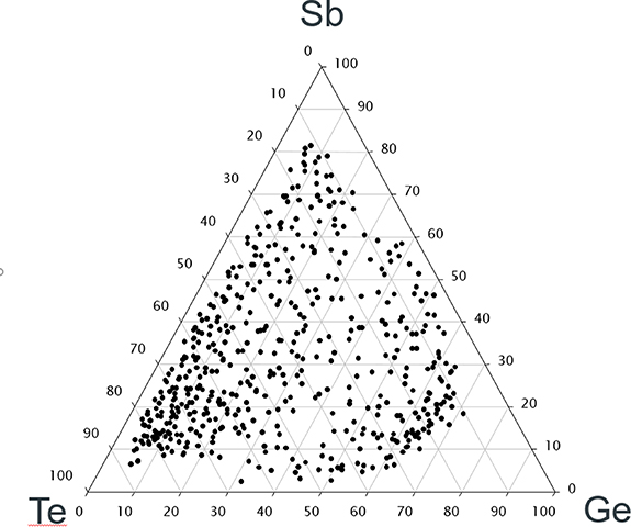
Figure 3. Mapping of a complete evaluation of the GST system, deposited by PVD on five substrates using high-throughput methodology, as described in Guerin et al [31].
Download figure:
Standard image High-resolution imageAdvances in science and technology to meet challenges
Clearly, by adopting high-throughput methodology in the search for chalcogenide alloys optimal for a given application, the volume of raw data generated is very large and therefore a current challenge is the development of new techniques for data management and processing. Two areas in which technological advances are meeting these challenges, or more appropriately, further enhancing the potential of high-throughput discovery of chalcogenide alloys, lie in expansion of the material library and collective database, and in the interpretation and use of the data within these.
It is logical to link high-throughput methodology and artificial intelligence tools, and this has been the case in recent years. Initially, computational resources were limited and so compromises were required both for performing the desired measurements and the subsequent data analysis. Advances in computing power increased the attractiveness of this approach and the use of advanced data analytics and applications of statistical and ML approaches to materials science is experiencing considerable growth. The growing library data both enables classical correlative ML, and also opens the pathway for exploration of underlying causative physical behaviors, as schematically shown in figure 4 [35–37].

Figure 4. From [37], the integration of theory databases, combinatorial libraries and imaging is key to the enabling unprecedented growth of material science allowing the combination of data to accelerate the understanding and development of new materials in next-generation devices and system, a data-driven future for which we expect chalcogenides to play a significant role.
Download figure:
Standard image High-resolution imageThese developments point towards a data-driven future wherein knowledge can be labeled, aggregated, and used collectively, accelerating the advancement of materials science. Artificial intelligence can be transformative not only in that it can allow for acceleration of scientific discoveries, but also that it can change the way materials science is conducted. Combining the available experimental and theoretical libraries in a physics-based framework can accelerate materials discoveries, and lead to lasting transformations of the way materials science research is approached worldwide.
Concluding remarks
The chalcogenide family, combined with their vast scope for compositional modifications and an accompanying wide range of active and passive physical properties, anchor chalcogenide alloys as enabling optoelectronic materials. Today, advancement in their application will benefit both from a thorough understanding of the underlying fundamental properties and the underlying causality, along with intelligent and automated direct assessment of the material family through high throughput methodology. Advances in ML tools are enabling the increased generation of databases and facilitate rapid prediction of properties, now quickly spanning the gap between fundamental material properties and the ultimate application, enabling more efficient design cycles for similar material systems.
Acknowledgments
The support of the UK's Engineering and Physical Science Research Centre is gratefully acknowledged through research Grant EP/G060363/1 entitled 'Manufacturing and Application of Next Generation Chalcogenides' and through the JIF Scheme (GR/M88365/01) for the Combinatorial Centre of Excellence in the School of Chemistry in the University of Southampton.
5. Development of switchable layered chalcogenides for photonic integrated circuit (PIC) applications
Yifei Li, Seong Soon Jo and R Jaramillo
Department of Materials Science and Engineering, Massachusetts Institute of Technology, Cambridge, MA 02139, United States of America
Status
Materials featuring switchable changes in optical refractive index are of prime importance for emerging and future systems including reconfigurable PICs for datacom and neuromorphic processing. PIC technology has achieved a remarkable level of maturity. Highlights include quantum emitters, neuromorphic computing accelerators, and phased arrays for beam steering. However, in key respects we remain at an early stage of development. We have not yet developed materials to enable strong optical phase modulation with the speed, insertion loss, power consumption, endurance, and process compatibility needed for future, fully-integrated photonic circuits, processors, and sensors. A particular need that arises in the context of optical data processing and neuromorphic computing is for multi-level optical phase modulation. Much research on compact multi-level optical phase modulators is focused on established PCMs in the GST alloy system. These materials benefit from decades of continuous development, but suffer drawbacks in terms of switching speed, optical loss, fatigue, and thermal management.
Current and future challenges
Before proceeding, we clarify the word 'phase'. In optics, the phase of light describes a relative position in a cyclic waveform. In materials science, the phase of a material is defined by its composition and structure, and determines its properties. Optical phase modulators change the phase of light relative to a reference beam. However, 'phase change' may also imply functionality deriving from a materials phase transformation, such as crystalline–amorphous transformations in GST, or martensitic transformations in TMDs. In an attempt to reduce confusion, throughout this document we use the term 'optical phase' to refer to the phase of light, and 'phase change' to refer to a materials phase transformation.
TMDs are layered, van der Waals-bonded solids with intriguing physical properties that include layer number-dependent band gap, electron pseudospin, exciton and trion excitations, wide chemical tunability, catalytic activity, and strong above-band gap light absorption. TMDs interact strongly with light and have large refractive index, yet can feature low loss for below-band gap photon energy [38, 39]. TMDs feature a panoply of polymorphs with contrasting electrical and optical properties, and in recent years there has been sustained interest in using TMD transformations for electronic device technology, although in many cases the underlying switching mechanisms remain unclear [40]. These transformations can be triggered by electric fields, charge injection, electrochemical reactions, and strain [41–44]. The availability of non-thermal switching mechanisms is exciting for fast and low-power switching. The small and collective atomic displacements during switching (figure 5(a)), facilitated by the layered crystal structure, suggest that material fatigue may be lower than for devices based on mass transport or PCMs. For instance, transitions between the 2H and 1T structure types can be described by a simple translation of a plane of chalcogen atoms, facilitated by an intermediate ripple in bond angles [45, p 2].
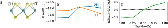
Figure 5. Atomic image and thermodynamics of 2H-to-1T phase transformation in TMD alloys. (a) Schematic diagram of MoS2 switching between 2H and 1T phases. (b) Theoretically predicted Gibbs free-energy ( ) at 300 K versus composition of 2H and 1T phases in the (Mo, Zr)S2 system.
  is calculated relative to isolated atoms in a vacuum, and includes calculations of phonon entropy and optimization for volume [38]. (c) Difference in free energy between 2H and 1T phases. In (b) and (c), the points are calculated data and the straight lines are guides to the eye.
Download figure:
Standard image High-resolution imageSwitching energy and speed are essential metrics for the proposed applications of TMD phase transformations. Theory predicts that, as a rule, the thermodynamic energy differences between polymorphs decreases on moving from sulfides, to selenides, to tellurides; these energy differences can also be tuned by alloying (figure 5(b)) [43]. However, these predictions have not been experimentally verified, and the transformation energy barriers—that will determine the operation of future devices—remain unknown. The fundamental limits on switching speed are also unknown. Temperature-driven structural phase transitions are sluggish, and can take minutes to hours even at temperatures well above 400 °C [45]. On the other hand, electric field-driven switching has been observed on the order of 10 ns (100 MHz) at room temperature [41]. Since the transformations involve coherent atomic-scale displacements, and do not require thermal activation or atom diffusion, it is reasonable that the fundamental speed limit would be that of phonon vibrations (THz).
Advances in science and technology to meet challenges
Thus far, the scientific community has focused mostly on demonstrating novel phenomena in model systems, not on optimizing materials for practical applications. Recent results suggest that TMD alloys will enable co-optimization of switching performance metrics including speed, energy, and retention [38, 41, 46]. This tracks the history of the development of more mature systems of active materials, such as GST, for which alloy design has been critical to move from demonstration to proven technology [47]. The history of mature PCMs illustrates that materials design plays an essential role in developing active, switchable materials. Layered materials offer a tremendous materials design space [40]. Now is the time for a strategic effort to optimize layered materials for optical phase modulation and PIC applications.
We end this section with a note on material form factor and crystallinity. Much research on TMDs prioritizes single crystals, either as bulk samples, exfoliated flakes, or epitaxial thin films. Such form factors are likely essential for applications in digital electronics, such as transistors based on TMD channels. However, for PIC applications, we see opportunity for polycrystalline films with thickness in the approximate range of 1–10 nm (i.e. many layers thick). Here we list four reasons why polycrystalline films may be preferred over single crystal flakes and films for controlling optical phase in PIC devices. (a) Grain boundaries accelerate the kinetics of martensitic transformations by providing nucleation sites such as defective edges. (b) Grain boundaries reduce the stress and elastic energy associated with martensitic transformations, because they contribute a free volume that is not available in single crystals. (c) The proposed optical phase shifters require sufficient volume of interaction between the optical field and the active material to enable PIC integration with devices on the  m scale. For instance, devices based on phase change GST typically use a film thickness of 10 nm of more, and our simulations show that TMD films of similar thickness will be effective as optical phase shifters in devices such as ring resonators [40]. In contrast, simulations show that monolayer TMD films with thickness under 1 nm have insufficient interaction volume to achieve useful optical phase change, even with operating near an exciton resonance that can be substantially modulated [40]. (d) Our experimental measurements (figure 6) suggest that chemical impurities contribute far more to parasitic, sub-band gap optical absorption than do grain boundaries. In other words, we can achieve low-loss material with film synthesis methods and pure precursors typical of electronic materials manufacturing, even with polycrystalline films with a high concentration of grain boundaries.

Figure 6. Near infrared loss index  (1500 nm) of MoS2 bulk, geological crystal, and synthetic, polycrystalline thin films. (a) Photograph of crystal used for spectroscopic ellipsometry measurements. (b) Micrograph of Si3N4 ring resonator with integrated MoS2 thin film. (c) Micrograph of Si3N4 waveguide with integrated MoS2 thin film. In (b) and (c) the patterned MoS2 films are only barely visible. The devices were made using conventional planar processing, combined with low-temperature, large-area TMD synthesis methods.
Download figure:
Standard image High-resolution imageConcluding remarks
The future is bright for PICs to enable faster and lower power computing, communication, and sensing than is possible with present-day electronic technologies. Phase change chalcogenides—including layered and two-dimensional TMDs—are promising as active materials in optical phase shifters, but turning this promise into commercial reality will require continued, focused R&D. The electrically triggered phase change functionality reported in monolayer and few-layer TMD crystals needs to be more widely reproduced and studied. The opportunities for alloy design and optimization described above should be pursued, so that trade-offs between switching speed, energy, and retention can be quantified and materials selection for device engineering can be placed on a firm footing. The impact of grain boundaries and crystal quality on materials performance and device longevity should be thoroughly studied. Beyond these materials-centric issues, there are worthy open challenges in device design and manufacturing, including electrode design, and the integration of TMD thin-film processing with established PIC foundry workflows.
Acknowledgments
This work was supported by an Office of Naval Research MURI through Grant #N00014-17-1-2661. We acknowledge technical assistance from Prof. Juejun Hu at MIT, and Prof. Mo Li and Changming Wu (University of Washington).
6. Interfacial phase change materials (iPCMs) and superlattices
Robert E Simpson1 and Junji Tominaga2
1 Singapore University of Technology and Design (SUTD), Singapore
2 National Institute of Advanced Industrial Science and Technology (AIST), Tsukuba, Japan
Status
Chalcogenide PCMs exhibit a radical change in their electrical and optical properties when switched between different structural phases, typically amorphous and crystalline. The switch is non-volatile, and no energy is required to maintain the state. The most studied and successful PCMs exist along the Sb2Te3–GeTe compositional tie line [48]. However, for many applications the energy required to switch these materials is too high. Although compositional tuning, doping, and alloying have been used to improve the energy efficiency of these PCMs, these methodologies cannot easily be generalized, which is important for designing PCMs with specific properties. In contrast, rather than alloying Sb2Te3 with GeTe, developing PCM superlattices by layering crystals of Sb2Te3 and GeTe allows the resultant properties to be tailored.
Sb2Te3–GeTe superlattices, which are also known as iPCMs [49], confine the phase transition to a plane at the Sb2Te3–GeTe interfaces. This reduction in dimensionality from the 3D phase transition seen in the Sb2Te3–GeTe alloys to 2D planes lowers entropic losses and concomitantly reduces the energy to switch the state of the material. Over the past decade iPCM electrical memory has been developed that switches with three orders of magnitude lower energy than its alloy counterparts [50].
The breakthroughs in the iPCM design stem from simplified models of the switching process and using them to optimize the structure in silico. Indeed, the superlattice platform is ideal for design because both the macroscopic and microscopic properties depend on the superlattice layered structure, which can be modeled using DFT with relatively small simulation cells. These computer models serve as a blueprint for the crystal growth. The superlattices that have been designed thus far all use a hexagonal unit cell with the (00l) planes parallel to the substrate. Practically, these structures are grown by high- temperature sputtering, pulsed laser deposition, or MBE.
Although the iPCM does exhibit large changes in optical properties, until now these efficiently switching superlattices have not been optimized for photonics applications. We see developing superlattices and iPCM specifically for photonics as the next stage of development with several potential application opportunities, see figure 7.

Figure 7. The iPCM superlattices are composed of GeTe and Sb2Te3 crystalline layers. Their efficient switching ability and programmable optical constants will make them the ideal for memory elements in future reprogrammable photonics on chip technologies. Moreover, their non-trivial electronic band structure is expected to enable new devices that exploit electro-photonic spin control.
Download figure:
Standard image High-resolution imageCurrent and future challenges
The biggest challenge facing iPCM photonics is the lack of published optical constants for the superlattice structures in both structural states. Although the as-deposited SET state can be readily studied by ellipsometry. The RESET state requires delicately switching an area sufficient for ellipsometry without destroying the superlattice layers.
Several reports suggest that the GeTe and Sb2Te3 superlattice layers interdiffuse [51, 52]. The effect of interdiffusion on the switching performance is unknown. The interdiffusion issue makes the growth temperature and method critical. Widening the growth temperature window by improving the stability of the superlattice will enable fabrication by the wider research community, and by conformal deposition methods, such as chemical vapour deposition and atomic layer deposition, which is important for creating high aspect ratio photonics devices.
Despite the radical improvements in switching efficiencies demonstrated in iPCM electrical memory, the thermal conductivity of the superlattice RESET state is higher than its equivalent alloys [49]. If the superlattice thermal conductivity could be lowered, then lower power heat pulses could be used to switch the material. For PCM programmed plasmonics and Si photonics, the surrounding materials tend to have a very high thermal conductivity that conducts heat away from the PCM. This means either engineering low thermal conductivity surroundings or engineering iPCMs with a lower thermal conductivity must be developed to further improve the switching efficiency.
The iPCM superlattice is also a topological insulator. Recently, the iPCM spin diffusion length at room temperature was estimated to be more than 100 μm, which is more than 100-fold longer than that observed in normal semiconductors [53]. This means that the topologically protected spin controllable area is far larger than a laser focal spot. We believe, therefore, that the iPCM is the ideal platform to design new electro-photonic spin control devices that enable left- and right-handed molecular selection, magneto-optic sensing, near-field spin isolation for post-5G and -6G communication devices, and temporary spin storage in quantum computing.
Advances in science and technology to meet challenges
The iPCM needs to be switched into the reset state for the optical properties to be studied. The easiest way to do this is via short pulse laser switching. Switching large areas of the material will also enable other experiments on the structure of the RESET state, such as x-ray absorption, to be conducted. These studies will, in turn, allow more accurate models of the switching process to be developed, which could lead to multi-level iPCM structures.
The stability of the superlattice can be improved by doping the layers [54] to inhibit the Sb double layers forming [55]. Recently, it was shown that replacing 3% of the tellurium atoms with sulfur in the GeTe superlattice layer improves the stability of the Sb2Te3–GeTe superlattices [53]. On one hand, it is important to stabilize the superlattice layers against interdiffusion but, on the other hand, we need to ensure that the superlattices can still efficiently switch. Therefore, switching time and energy studies must also be performed on these new doped materials.
Thermally engineering superlattices with lower thermal conductivity is currently being researched [56]. Amazingly, the thermal and electronic conductance normal to the iPCM layers are, respectively, four- to 16 times and 2000 times lower than the in-plane direction, which is due to the van der Waals gap [56]. Therefore, removing intermixing from the interfaces and designing a perfect superlattice structure can further lower the thermal conductivity. Again, we also believe that doping or alloying these layered materials is a promising approach to further lower the thermal conductivity. To increase the switching efficiency of phase change photonics devices, new materials that can increase the thermal boundary resistance using the van der Waals effect without influencing the optical response must also be developed; perhaps ultra-thin thermal barriers with a lower refractive index are the answer. Further improvements may be gained by using non-thermal phase transitions, which have already been demonstrated in TMD materials by combining them with a ferroelectric substrate [57]. Since the iPCM superlattice switching energy scales with strain, we suspect a similar approach can be used to switch it. Moreover, GeTe is ferroelectric, and therefore could enable the GeTe layers to switch directly by combining heat and electric fields.
Concluding remarks
The recent explosion of research in PCM programmed photonics mostly exploits the well-known data storage PCMs, such as those along the GeTe–Sb2Te3 compositional tie line. However, the iPCM and chalcogenide superlattices open a new possibility to design bespoke materials for different photonics applications. Moreover, these superlattices exhibit properties that are unseen in their alloy counterparts, such as topologically non-trivial electronic band structures. We foresee, therefore, these materials not only being used to increase the efficiency of phase change photonics designs but also fuelling a field of reprogrammable novel spintronic-photonics.
Acknowledgments
The research discussed in this section was funded by the A*Star Nano Spatial Light Modulators Program (A18A7b0058), the Singapore Ministry of Education (MoE 2017-T2-1-161), the Office of Naval Research Global (N62909-19-1-2005), and the Japan Science and Technology Agency (CREST-JPMJCR14F1).
7. Chalcogenide metamaterials and metasurfaces
Yihao Cui, Avik Mandal and Behrad Gholipour
Nanoscale Optics Lab, Electrical and Computer Engineering Department, University of Alberta, Edmonton, Canada
Status
Since the dawn of the century metamaterials and metasurfaces have emerged as highly promising candidates for integration in various nanophotonic device platforms due to their design versatility and scaling potential. Artificial resonant electromagnetic media nanostructured on the subwavelength scale; they are an emerging technology paradigm for engineering electromagnetic space and controlling the propagation of light and its interaction with matter. An extensive range of enhanced and unusual optical properties, including dynamically tuneable/switchable and nonlinear functionalities, have been demonstrated at technologically important near-IR and visible frequencies, in metamaterials and metasurfaces comprised of nanostructured plasmonic metals (very typically gold or silver), high-index dielectrics (often silicon, but also GaAs, transparent conductive oxides, germanium, perovskites and chalcogenides) and metal/dielectric composites. The current evolutionary stage in this burgeoning field is advancing it from being a nanotechnology-enabled paradigm for engineering passive electromagnetic properties to the adaptive and field-programmable device and system levels that operate in dynamic real-world environments.
To this end, in the last decade various reconfiguration mechanisms inherent to different material platforms have been explored including thermo-optic effects, nano-optomechanical nonlinearities as well as free-carrier-modulation in graphene, silicon and transparent conductive oxides to name a few. Amongst these material platforms, chalcogenides (alloys of sulfur, selenium and tellurium) provide a promising route to the realization of a range of optically reconfigurable devices. While many are topological insulators or can be fabricated as monolayers, and so have the potential for extreme scaling, they are also CMOS compatible through their traditional use in optical disc (e.g. Bluray) and electronic PCRAM platforms. They also exhibit very large optical nonlinearities alongside a reversible, non-volatile switching capability between their amorphous and crystalline phases which can be instigated through optical, electrical or thermal stimuli. These two phases exhibit a unique plasmonic to dielectric transition across visible frequencies for certain stoichiometries and a high contrast in optical constants (Δn > 1) over telecom frequencies. Notably they can be switched with pulses down to the femtosecond timescales in binary or multi-level (grayscale) regimes.
Due to the plethora of intriguing properties exhibited by phase change chalcogenide alloys, their integration within various nanophotonic metamaterials, metadevices and metasystems has ignited intense research interest worldwide. An ever-expanding array of functionalities is being demonstrated almost daily, enabling non-volatile control of intensity, phase and polarization of incident light from ultra-violet to microwave frequencies [58, 59], unlocking a variety of metaswitches for dispersion control, aberration-free metalenses with switchable focal points and tunable beam steering metamaterials for wavefront control (figure 8). Device architectures in this domain either hybridize the phase change layer with a plasmonic metal or high-index dielectric resonator or utilize an all-chalcogenide approach. The former design involves decoupling the resonant component from the reconfiguration mechanism by integrating a high-index phase change chalcogenide component in the near-field of a plasmonic or dielectric resonator, while the latter takes advantage of the ultra-high refractive index of many phase change chalcogenide alloys to enable high-quality factor Mie resonances, mostly across IR frequencies. Here, the transition from amorphous to crystalline phase in the chalcogenide layer brings about a dramatic change in the resonant properties of a metamaterial or metasurface. In most alloys this involves a red-shifted spectral response and lowering in the quality factor of the resonance resulting from the higher refractive index and extinction coefficient associated with the crystalline phase (figure 9).
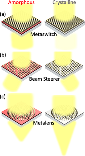
Figure 8. Phase change chalcogenide metamaterials and metasurfaces are being explored globally as non-volatile ultrathin (a) optical switches and modulators (metaswitches), (b) phase gradient beam steering metasurfaces and (c) reconfigurable metalenses.
Download figure:
Standard image High-resolution image
Figure 9. (a) Typical structure of (i) hybrid and (ii) all-chalcogenide phase change metamaterials and metasurfaces, where (b) a reversible amorphous to crystalline phase transition brings about drastic changes in the (c) resonant response of the metadevice.
Download figure:
Standard image High-resolution imageCurrent and future challenges
Phase change chalcogenide semiconductors have traditionally been used in data storage applications where the requirements in endurance switching of such devices is lower in comparison with applications that are currently being explored for phase change nanophotonics where in the context of signal modulation in telecommunication networks or display technologies endurance switching on the order of >1012 cycles are very typical. Therefore, a global effort is currently underway and justifiably gaining momentum to explore various mechanisms and device configurations to reduce the drift and noise associated with repeated switching events while enhancing the cyclability limit of these alloys. In the case of metamaterials and metasurfaces, due to the larger lateral footprint of such devices arising from their reliance on collective resonances, the challenge in low noise and drift, endurance cycling is compounded as transitions over relatively large micron-scale lateral areas is typically pursued as compared to the small nanoscale vias used in electronic PCRAM devices.
As this technology platform matures more emphasis will have to naturally be placed on packaging and integration of the developed devices into existing and emerging computing and telecommunication networks reliant upon optical fiber/waveguide architectures [60]. Furthermore, GST has been a traditional material of choice in these devices. However, due to the inherent losses of this semiconductor at visible and telecommunication frequencies, there is an on-going search for new alloys with more favorable extinction coefficients across commercially important spectral bands. More recently, the identification of selenium- and sulfur-based alloys (e.g. GSST, SbS or SbSe) with lower optical losses has been a welcome addition [47, 61]. However, many intriguing aspects of their performance such as switching speed limits, endurance cycling, grain sizes and chemical/environmental stability are yet to be fully understood and therefore remain active areas of research.
Finally, it should be noted that the chalcogenide alloys have many overlooked volatile and non-volatile transitions ripe for exploration as alternatives to phase change [62]. For instance, a severely overlooked property of metal-doped amorphous chalcogenide semiconductors, in particularly certain sulfides and selenides, is that they exhibit directional photo-induced long-range movement of their constituent metal ions when exposed to light with a photon energy equivalent or higher than the optical band gap of the chalcogenide. This 'photo-ionic' movement can result in substantial and non-volatile changes of material properties (refractive index and conductivity) at the nanoscale facilitating robust, low power, non-binary dynamic molding of light [63]. Such alternative non-volatile effects that operate without the need for a power-hungry melt–quench process inherent to phase change should be explored further.
Advances in science and technology to meet challenges
The chalcogenide alloys exhibit compositionally tunable optoelectronic properties that can be stoichiometrically engineered at specific frequencies through emerging high-throughput combinatorial material discovery techniques [64]. In the hunt for a low optical loss, fast-switching alloy with universal endurance, the wide adoption of this technique for the identification of precise compositions is essential in accelerating advances on this front.
The thermal origins of the phase transition imply that precise control of heating/cooling rates is a necessity in designing devices for emerging telecommunication and computing applications with strict operational metrics. Switching speeds, modulation contrasts and endurance are a strong function of device architecture in phase change chalcogenide metadevices [65, 66]. Therefore, aside from the need to develop mass-manufacturable fabrication and packaging techniques that enable nanofabrication of intricate nanostructures on the tips and sides of optical fibers platforms, this will also necessitate development of new theoretical and simulation frameworks that couple thermal, optical and electronic physics for precise design of the temporal switching response of such devices.
Although a large number of all-optical devices have been demonstrated globally, in the short to medium term the design of electro-optic devices is essential for integration with existing computing and telecommunication platforms. Here, resistively switching through the chalcogenide layer does not provide a homogenous phase transition desirable for nanophotonic device platforms due to filamentation effects. To produce spatially homogenous phase transitions, the emergence and use of micro/nano-heaters is rapidly becoming the preferred method of electrically addressing these devices, where advances in nanoheater designs will have direct impact on improvements in switching energies and speeds.
Conclusion
Chalcogenide phase change metamaterials and metasurfaces hold the key to major breakthroughs in a variety of different optoelectronic device applications that require adaptive responses relying on field-programmable reconfiguration. We envision that the rapidly progressing understanding of the fundamental physics of phase change nanophotonic devices in particular for metamaterial and metasurfaces, together with the ongoing development of specialized stoichiometric engineering and device fabrication and packaging technologies, will lead to the establishment of a uniquely flexible CMOS compatible platform capable of integration with existing and emerging network and computing architectures.
Acknowledgments
The authors would like to acknowledge support from the Canadian Natural Science and Engineering Research Council (NSERC) and Alberta Innovates (No. 202102642).
8. Chalcogenide nonlinear optical photonic circuits
Benjamin J Eggleton
School of Physics, University of Sydney Nano Institute (Sydney Nano), University of Sydney, Sydney, NSW 2006, Australia
Status
Since the early 2000s there has been a renaissance in nonlinear optics research and technology, particularly in the context of signal processing and light source development [67–70]. ChGs, which have unique nonlinear optical properties, have played a key role in this renaissance and are well placed to deliver new technological solutions. The most striking property of the chalcogenides are the ultra-strong third-order optical nonlinearities which can be as high as 1000 times that found in silica. Being based on amorphous material, the ChGs offer a pure optical nonlinearity, largely absent of free-carrier absorption, thus the nonlinearity is essentially instantaneous and has negligible nonlinear losses. Strong optical nonlinear processing functions have been demonstrated in optical fibers, including supercontinuum generation, frequency conversion, and optical switching. When combined with the transparency of ChGs into the mid-IR wavelength region, there is then prospect for very broad band coherent light sources, having important applications in spectroscopy for environmental monitoring and health sciences. Finally, it is worth noting the ChGs are photosensitive which provides a degree of freedom to post-tune the optical properties although this can come at the expense of stability.
The development of photonic chip-based chalcogenide waveguides combining strong optical nonlinearity and mid-IR transparency with the compactness and ultrahigh confinement offered by photonic integration technology offers a paradigm shift in the development of compact light sources, signal processing, and sensor technologies. It is particularly well-suited for applications requiring reduction in size, weight, and power consumption [69–71]. Chalcogenide photonic circuits have been demonstrated for broadband supercontinuum generation [71] and parametric processing based on four-wave-mixing for applications in telecommunications [69–71] and the generation of correlated photonics for quantum photonics applications [69, 70]. Related to the strong third-order nonlinearity, the Raman and Brillouin gain coefficient is hundreds of times larger than that provided by silica waveguides, thus providing possibilities for Raman and Brillouin gain-based devices.
The strong Brillouin gain of ChG is sufficient for efficient interactions on the centimeter-length scale [72, 73], and has already been the basis of novel chip-based narrowband optical filters [74], phase shifters, and delay elements. They have also been extensively developed for applications in microwave photonics. Brillouin integrated photonic circuits based on chalcogenide waveguides represent a new paradigm in chip-based signal processing offering a unique advantage with respect to silicon waveguides, in which Brillouin interactions are limited due to the nonlinear loss and acoustic confinement of silicon. Below we expand on these recent developments and highlight opportunities for further development and potential technological advances.
Current and future challenges
SBS in waveguides depends on several conditions being met, most importantly it scales strongly with the refractive index of the material [73]. For this reason, the ChGs, which have an index of around 2.5, have a Brillouin gain coefficient roughly about 100 times larger than that of the silica itself. Combined with the strong optical mode confinement offered in chalcogenide planar waveguide circuits, massive Brillouin gain is possible. Achieving strong Brillouin gain, however, also depends on acoustic confinement, which is particularly important in waveguides with dimensions comparable to the wavelength [72–76]. Acoustic confinement depends on the speed of sound in the core region, relative to the speed of sound in the cladding region. When the speed of sound in the core is lower than that in the cladding, which is indeed the case for chalcogenide surrounded by silica, then the acoustic mode is confined and does not leak. This is analogous to the concept of total internal reflection for lightwaves. This in turn translates into good overlap between the optical and acoustic modes, leading to strong SBS. This contrasts with the case of silicon on silica, wherein the acoustic modes are leaky and dissipate on timescales comparable to the phonon lifetime, thus inhibiting the SBS gain. As outlined in figure 10, the first demonstration of on-chip SBS which was reported using an As2S3 planar waveguide achieved 15 dB of gain using about 100 mW of pump power [73]. Subsequent optimization of the cladding geometry led to significant increases in the SBS gain to levels of 55 dB [75].

Figure 10. Evolution of chalcogenide PICs in the last decade: (a) original demonstration using rib waveguides [72]; (b) in optimized waveguide geometry for enhanced acoustic confinement [73] and (c) hybrid integration in CMOS compatible silicon circuit [74].
Download figure:
Standard image High-resolution imageThe SBS gain response provides an exquisite resonance approximately 20–30 MHz wide which is almost perfectly matched to the needs of important microwave filter and sensor applications [75]. When combined with bias optimization techniques using Mach Zhender modulators, ultra-deep notch filters, as shown in figure 11, can be achieved with only modest pump power, allowing us to avoid operating the chalcogenide waveguides in regimes where photostability issues exist [75]. On-chip SBS also offers other important functionality, including light storage and control of phase and true-time delay which in turn relies on strong SBS gain and high pump power. Ensuring the stability of ChGs remains the most significant challenge. The difficulty revolves around the need to identify a glass composition that has both the required stability for high optical fluence while at the same time is suitably nonlinear and transparent. Further development of the chalcogenide waveguide platform requires the integration of other passive and active components, many of which are already available through CMOS photonics foundries. Examples being optical modulators, photodetectors, lasers, and non-reciprocal functionality [74, 76].
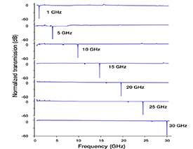
Figure 11. Frequency agility of microwave photonic notch filter implements using SBS in chalcogenide PIC [75].
Download figure:
Standard image High-resolution imageAdvances in science and technology to meet challenges
The key challenge for on-chip SBS is the development of mechanically robust waveguide systems that can jointly confine light and high-frequency acoustic phonons in an easily manufactured and CMOS compatible platform [75, 76]. Our approach has been to pursue a hybrid integration platform that incorporates chalcogenide waveguides into a CMOS compatible silicon photonic circuit [74]. In this approach, a silicon photonic circuit is manufactured using traditional CMOS deep UV lithography, allowing for the incorporation of passive components and active components. It is subsequently etched to allow for deposition of As2S3 and lithographically defined waveguides [74]. The chalcogenide waveguides are seamlessly interfaced with the silicon waveguides using an inverse taper structure that has remarkably low loss. Using this approach, we fabricated a compact spiral device within a silicon circuit, achieving 15 dB of SBS gain, notably this is almost an order-of-magnitude improvement in Brillouin amplification relative to published silicon chips. To establish the flexibility of this approach, we fabricated a ring resonator with a free spectral range precisely matched to the Brillouin shift, enabling the first demonstration, to our knowledge, of Brillouin lasing in a planar integrated circuit [74]. Subsequently, we demonstrated a circulator-free Brillouin photonic circuit based on a backward inter-modal Brillouin scattering in a multi-modal waveguide. Conveniently, this allowed for the separation of counter-propagating pump and signal using passive integrated mode-selective filters incorporated into the surrounding CMOS compatible silicon circuit [76]. These demonstrations highlight the potential for hybrid integration to ultimately achieve a fully integrated device that has the size, weight, and power requirements for deployment in mobile applications. We recognize that further integration is required, particularly the integration of the active optoelectronic components, such as the laser, the modulator, and the photodetector. Fortunately, there is already excellent progress and development in these parallel fields, motivated by the demands of telecommunications networks and data centers. High-bandwidth modulators are already being implemented in CMOS compatible silicon waveguides, exploiting free carriers, and are readily available through silicon photonic foundries, such as IMEC. Stability and the lifetime of the ChGs continues to be a priority, but significant progress has already been made in the packaging and preparation of these devices that bodes well for future deployment.
Concluding remarks
Chalcogenide waveguides have enabled a renaissance in nonlinear optics as they offer pure ultrafast third-order nonlinearities which are ideal for signal processing. Further enhancements have been realized through the development of microstructured optical fibers and integrated circuits where waveguides designed to engineer and tailor the dispersion properties lead to efficient parametric interactions and supercontinuum generation. The discovery of on-chip SBS has opened a new frontier in microwave photonics and sensing applications and is promoting further developments in hybrid integration technology to enable SBS devices to be fully integrated. Chalcogenide photonics continues to be researched in laboratories around the world with efforts primarily focused on tailoring their composition to enhance optical nonlinearities.
Acknowledgments
The author acknowledges the contributions of many staff, students, and collaborators as well as funding agencies, particularly the Australian Research Council that have supported this body of research.
9. Fiber optics technologies for the mid-infrared (IR)
Martin Rochette, Mohsen Rezaei, Imtiaz Alamgir, Mobarok Shamim, Robi Kormokar, Arslan Anjum and Gebrehiwot Tesfay Zeweldi
Nonlinear Photonics Group, McGill University, Montréal, Canada
Status
The mid-IR spectrum of light (2–25 µm) is a topic of technological excitement and growing research activity. For instance, chemical substances exhibit vibrational and rotational absorption bands in the mid-IR, and the unique signature left by the absorption of light by these fundamental bands provides a universal means for their identification and quantification, with applications for medicine and biology, industrial processes, environment monitoring, defense, quantum optics, and imaging.
Despite holding a vast range of applications, photonics technologies in the mid-IR are just beginning to emerge with respect to widespread photonics technologies in the near-IR (0.7–2.0 µm). Near-IR technologies have bloomed thanks to fiber optics, a market that currently represents close to 1 billion USD yr−1, with rapidly evolving sectors of applications such as optical fiber communications, fiber lasers, and fiber-based sensors. The optical transmission of silica fiber, a fundamental component of fiber optics, is however limited to the spectral range of 0.4–2.0 µm, because of transmission losses that increase abruptly beyond those limits. Fiber optics in the mid-IR therefore require transmission media other than silica to become viable.
As of now, optical fiber components (e.g. optical fibers, beam splitters, and polarizers), optical fiber devices (e.g. interferometers and pulse characterization systems), and optical fiber sources (e.g. lasers, parametric oscillators, and supercontinuum sources) that operate in the mid-IR are rare, if existing, or lack technological maturity. Nonetheless, such mid-IR fiber optics technologies are in high demand to fulfill the wide technological gap with respect to near-IR technologies. Of particular interest are optical fiber components that enable the fabrication of devices and sources with better mechanical stability, lower optical losses, and robustness to environment than their free-space counterparts.
The basis of mid-IR fiber optics technologies having been set up, optical fibers made of soft glass such as chalcogenide and fluoride fibers of various geometries (e.g. step index, crystal fibers, and suspended core) have now reached sufficient maturity for commercialization. Those fibers currently find application in defense, astrophysics, and medical instrumentation and are destined to play a fundamental role in the development of fiber optics technologies in the mid-IR.
Current and future challenges
As of now, chalcogenide and fluoride fibers have been used, sometimes even in tandem, to demonstrate supercontinuum generation e.g. spreading over a spectral range of 2–10 µm [77, 78]. While the fluoride fiber triggers nonlinear effects from high optical intensity because of a relatively low optical nonlinearity (n2 = 2.1 × 10⁻¹⁶ cm2 W−1 ≅ n2,SiO2), the chalcogenide fiber triggers supercontinuum generation from low optical intensities thanks to its high nonlinearity (n2 = 2.5 × 10⁻¹³ cm2 W−1), but at the cost of a reduced damage threshold intensity with respect to fluoride fibers.
In addition to mid-IR compatible passive fibers, rare earth-doped fluoride fibers have also been used for the fabrication of lasers in the mid-IR [79]. Those lasers rely on the use of a fluoride fiber acting as the gain medium, surrounded by free-space optical components such as, for example, broadband and dichroic mirrors, a saturable absorber, and focusing lenses. The growth of fiber optics in the mid-IR therefore depends on the development of fiber-based components that will serve as building blocks for the fabrication of devices and optical sources. Chalcogenide and fluoride fibers appear to be the ideal starting point from which such components can be built.
Advances in science and technology to meet challenges
The development of mid-IR fiber optics components is currently the subject of intensive research activity. One such component, the chalcogenide optical fiber taper is most useful for tasks of nonlinear amplification and processing, with a nonlinearity enhanced by ∼104 times (thus γ ≅ 200 (W.m)−1) with respect to the single-mode chalcogenide fiber, and with a chromatic dispersion that is broadly engineerable from normal, to zero, to anomalous [80]. Chalcogenide tapers provide a solution for supercontinuum generation [78], wavelength conversion [81, 82], and optical parametric oscillation [83] with low power consumption.
Another recently developed component is the single-mode optical fiber coupler (OFC) [84]. A typical OFC is a 2 × 2 ports fiber device that combines the power from two fibers into a single one, or that splits the power of one fiber into two fibers. This power combination/splitting can be wavelength independent, wavelength dependent, or polarization dependent. Figure 12 shows the structure of a typical OFC (figure 12(a)) and their processing actions (figures 12(b)–(d)). Chalcogenide OFCs can be spectrally broadband and act as power divider/combiner, spectrally dependent and act as wavelength division multiplexers/demultiplexers, or they can be polarization dependent and act as polarization multiplexers/demultiplexers.

Figure 12. (a) Schematic of a tapered OFC. In (b)–(d), schematizing the processing action in the waist region of a coupler, leading to (b) broadband power divider/combiner, (c) wavelength division multiplexer/demultiplexer, and (d) polarization multiplexer/demultiplexer.
Download figure:
Standard image High-resolution imageWith the growing availability of optical fiber building blocks compatible with the mid-IR such as optical fibers, fiber tapers, OFCs, optical fiber saturable absorbers [85], and certainly many others to come, it is expected that all-fiber devices and all-fiber light sources will quickly develop. Just recently, the first all-fiber chalcogenide ring laser has been demonstrated [86]. It consists of a combination of an As2S3 optical fiber for nonlinear amplification and of an As2Se3 OFC to close the resonant ring cavity, inject pump power, and extract laser power. The amplification mechanism is the spectrally strong and narrow Brillouin gain, which enables the laser to be used as a coherence enhancing device. Pumped with a laser at a wavelength of 1550.45 nm and linewidth of 14.4 MHz, the Brillouin laser oscillates at a wavelength of 1550.52 nm with a linewidth of 1.9 MHz, thus providing coherence enhancement by a factor of >7. Figure 13 shows a schematic of the all-fiber chalcogenide ring laser. Probing the Stokes power as a function of pump power (figure 13(b)) provides a laser threshold evolution. The Stokes spectrum is clearly visible from the output spectrum of the laser (figure 13(c)) when pumped above threshold.

Figure 13. (a) Schematic of the all-fiber chalcogenide ring laser. PC: polarization controller; OC: optical circulator; OSA: optical spectrum analyzer; OFC: optical fiber coupler. (b) Stokes power as a function of pump power delivered to the input of ring cavity. (c) Optical spectra of the bi-doped fiber laser for a pump power below threshold (60 mW) and above threshold (73 mW).
Download figure:
Standard image High-resolution imageConcluding remarks
Fiber optics components, devices, and light sources that operate in the mid-IR are currently the subject of intensive research activity. Passive optical fibers made of chalcogenide and fluoride glasses, rare-earth doped fluoride glasses to act as gain media, optical fiber tapers, OFCs and many others are being developed to form building blocks of mid-IR fiber optics. Those components have just begun to be assembled into mid-IR fiber optic devices and light sources. It is thus expected that fiber lasers made of chalcogenide and fluoride fibers and components will be blooming in a near future.
Acknowledgment
This research is supported by the Natural Sciences and Engineering Research Council of Canada (NSERC).
10. Chalcogenide glasses (ChGs) for integrated photonics
Tushar Sanjay Karnik and Juejun Hu
Department of Materials Science and Engineering, Massachusetts Institute of Technology, Cambridge, MA 02139, United States of America
Status
ChGs have long been regarded as a promising material for integrated photonics given their exceptional IR transparency, large optical nonlinearity, ease of processing into a thin film form, and unique phase change behavior. Explorations of ChGs as an integrated optical waveguide material date back to the 1970s. Early investigations have placed significant emphasis on optically written waveguides in ChG films capitalizing on their photosensitivity—local refractive index change when exposed to light with near-band gap photon energies—while subsequent research pivoted towards adapting standard microfabrication techniques such as photolithography, wet and dry etching, lift-off, or nano-imprint to creating high-index-contrast, single-mode ChG waveguides [87].
The demonstration of low-loss ChG waveguides with strong optical confinement has already enabled a cohort of applications. The examples include ultrafast all-optical signal processing, where the large Kerr nonlinearity and low two-photon absorption of ChGs give rise to enhanced nonlinear figures-of-merit compared to Si. The broadband transparency of ChGs prompts their applications in spectroscopic chemical sensing, in particularly in the mid-IR spectral regime where characteristic absorption signatures of most molecules reside. Given this unique combination of superior nonlinearity and broadband transmission, ChGs also represent an ideal material choice for nonlinear frequency mixing via supercontinuum, frequency comb, or Raman/Brillouin amplification, allowing access to a wide range of wave bands outside the spectral coverage of conventional laser sources. The high refractive indices and substrate-agnostic integration capacity of ChGs facilitate hybrid integration with new materials such as electro-optic and magneto-optical crystals, flexible polymers, 2D materials, and semiconductor optoelectronics. Their photosensitivity has been exploited for post-fabrication trimming of photonic devices and more recently reconfigurable writing of photonic nanostructures. Finally, their large Brillouin scattering cross-section has led to the demonstration of on-chip microwave photonic filters with exceptional selectivity [75]. Besides leveraging their low-loss light transmission characteristics, the amorphous–crystalline transition of ChGs and the unusually large optical property modulation associated with the phase change further spurred their widespread use in reconfigurable photonics, photonic memories, and optical analogue computing during recent years.
Current and future challenges
As ChGs forge their path into mainstream integrated photonics, there are several challenges yet to be fully addressed as we elaborate below.
First and foremost, integration of ChGs with standard foundry-processed photonic platforms is the rational approach to expedite and expand their adoption in integrated photonics applications. The amorphous structure and low processing temperature of ChGs imply that they can be seamlessly integrated with other photonic components during backend processing. Indeed, monolithic backend integration of ChGs with foundry-processed silicon photonic devices has been reported by several groups [74, 88–91]. Moving yet a step further, in-foundry process integration of ChG photonics will be desirable to ensure consistent device performance. This however demands significant process development and is only possibly justified if any of the high-volume applications of ChG photonics come to fruition, for example, in neuromorphic photonic accelerators.
The performances of the ChG photonic devices will continue to improve. For most of the applications based on ChG waveguide devices, loss reduction is an unwavering pursuit (figure 14). These efforts should also be gauged in the context that other potential competing material platforms such SiN have achieved remarkably low losses down to the sub 1 dB m−1 level. In principle, ChGs can also reach a similar level of low attenuation, evidenced by the ultrahigh Q-factors (70 million) that have been measured in ChG microspheres [92], although processing innovations are mandated to attain comparable performances in on-chip platforms.
Figure 14. Propagation loss of waveguides fabricated with different material platforms. Data for ChGs (black, solid) [93–108], silicon nitride (red, open) [109–112], silicon (blue, open) [113–120], germanium (magenta, open) [121–130], III–V semiconductors (green, open) [131–136], and silver halides (violet, open) [137, 138] are given.
Download figure:
Standard image High-resolution imageExtending of the operation wavelength regime of ChG on-chip devices to the long-wave IR (LWIR, 8–14 μm) and beyond presents another research frontier. While ChGs' exceptionally wide IR transparency sets them apart from other materials such as Si and SiN, most efforts to date have been limited to ChG devices working in the near- and mid-wave IR ranges with only a few studies exploring even longer wavelengths.
Last but not least, as a class of 'soft glasses' characterized by low glass transition temperatures, ChGs reside in a thermodynamically metastable state and are susceptible to structural relaxation over an extended period of time or upon moderate heat treatment (e.g. during subsequent backend processing steps or solder reflow in chip packaging), causing non-negligible drift of their optical properties. Systematic characterization and mitigation of the resulting drift define the prerequisite to realizing robust ChG photonic device design.
Advances in science and technology to meet challenges
On the topic of foundry process integration, chalcogenides have already established a successful paradigm in the non-volatile memory industry. For instance, chalcogenides constitute the enabling material for Intel's XPoint memory: the phase change memory element is made of a GST alloy, and the selector is based on ovonic threshold switching of an As-doped Ge–Si–Se compound. Clearly, there is a viable (albeit challenging) path for integration of ChGs with mainstream photonic foundry manufacturing, even though one or more high-volume applications must be identified in the first place. Phase change photonics based on ChGs, which claims tantalizing prospects for programmable photonics and analogue computing, seems like a plausible candidate to motivate the effort (figure 15). To practice such integration, a series of rigorous tests must be performed to qualify the material for use in a foundry environment, including but not limited to maturing ChG deposition and fabrication procedures on the full-wafer scale, validating compatibility with various other processing steps, establishing compliances with occupational and environmental safety regulations, ensuring that the new material does not introduce harmful contaminants or compromise performance of other on-chip devices, and identifying suitable encapsulation layers to prevent undesirable interdiffusion, if deemed necessary. Along this line, we note that integration of low-loss chalcogenide phase change alloys with standard silicon photonic foundry processes has recently been demonstrated [139].
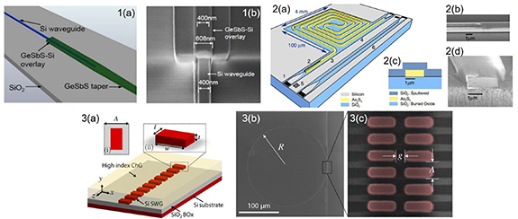
Figure 15. Backend integration of ChGs with silicon photonic devices. 1(a) GeSbS–Si hybrid adiabatic coupler (schematic). 1(b) GeSbS–Si hybrid adiabatic coupler (scanning electron microscope (SEM)). 2(a) As2S3–Si hybrid Brillouin device (schematic). 2(b) Si to As2S3 transition taper (SEM). 2(c) Cross-section of As2S3 waveguide (schematic). 2(d) Cross-section of As2S3 waveguide (SEM). 3(a) Silicon subwavelength grating waveguides (SWGs) with As20S80 cladding (schematic). 3(b) SWG mircoresonator (SEM). 3(c) Close-up of the coupling gap [74, 88–90].
Download figure:
Standard image High-resolution imageBenefitting from streamlined fine-line lithography and etching protocols, the optical loss of ChG waveguide devices has been decreasing steadily over the past few years. Reduction of losses to the <1 dB m−1 level, however, warrants innovative fabrication techniques. In particular, templated fabrication offers a promising route to create ultralow-loss ChG structures: ChG micro-resonators with an intrinsic Q-factor exceeding 10 million has recently been demonstrated using the approach. The templated fabrication technique can be coupled with thermal reflow or dewetting to further suppress scattering loss due to surface roughness. We anticipate that optimization of the templated fabrication route and other new process innovations will usher a new generation of ultralow-loss ChG devices critical to nonlinear optics and sensing applications.
ChGs with low phonon energies, in particular tellurides, boast exceptionally wide IR transmission extending well into the far-IR regime (>20 μm wavelengths). Devices operating in this wavelength range find applications in spectroscopic sensing, IR countermeasures, and astronomical optics, but are difficult to implement using alternative photonic materials. LWIR ChG photonics realized to date are exclusively fabricated on bulk ChGs. Transferring the devices to common substrate platforms entails development of new architectures exemplified by suspended waveguides to avoid radiative leakage loss. The suspended design also furnishes additional benefits in engineering modal dispersion and optical confinement.
Lastly, it is important to identify ChG compositions tailored towards enhanced thermal and photostability. Studies investigating the impact of thermal and/or optical treatment on glass structures are also warranted. Insights from the studies will rationally guide optimization of post-fabrication treatment protocols to stabilize glass film structures and minimize relaxation. Finally, quantifying the property drift of ChGs involves development of precision optical metrology techniques (e.g. resonant cavity refractometry [140]) commensurate with in situ measurement in manufacturing-relevant device settings.
Concluding remarks
ChGs offer a range of unique optical attributes and processing advantages for planar photonic integration. To fully unleash the potential of ChG photonics, several technical barriers must be overcome, including foundry process integration and continuing improvements of optical performance, spectral coverage, and device robustness. We are confident that thriving research and development efforts in this field will address these challenges in the coming years, enabling ChG photonics to make a major impact on integrated optics.
Acknowledgment
We acknowledge financial support from the National Science Foundation under Award No. 2024017.
11. Doped and alloyed amorphous selenium (a-Se) photoconductors in x-ray imaging detector applications
S O Kasap1, G Belev1 and A Reznik2
1 University of Saskatchewan, Saskatoon, Canada
2 Lakehead University, Thunder Bay, Canada
Status
The majority of flat panel x-ray imagers (FPXIs) used in mammography today, in one form or another, use doped and alloyed a-Se alloys [141–144]. There are at least four different technologies in the market (by Hologic, Analogic, Fuji, and KA Imaging) but all four are based on the x-ray photoconductivity of a-Se. Given the importance of x-ray imaging, a-Se has found a particular niche application in the mammographic modality due to three distinct advantages. (a) a-Se can be easily coated, by conventional vacuum deposition techniques, onto a large area with uniform and reproducible properties. The substrate temperatures are typically under 100 °C, which means a-Se can be easily coated onto thin-film transistor (TFT) active-matrix arrays on glass substrates to fabricate FPXIs, without damaging the TFT panels. (b) The dark currents that can be attained in multilayer a-Se device structures are under 0.1 pA mm−2. In a typical p–i–n-type a-Se detector, all layers are based on ChGs as shown in figure 16(a). (c) With appropriate doping, both hole and electron ranges (μτ products) lead to essentially near-unity charge collection efficiency. There are two exciting new developments. First, already commercialized by KA Imaging, is a-Se-coated CMOS chips that provide high-resolution imaging. Second is the use of the photoconductivity of a-Se in the visible range and avalanche multiplication in a-Se at high fields to fabricate large-array avalanche photodetectors [145, 146] to couple to a scintillator towards indirect medical imaging. Figures 16(a) and (b) illustrate a-Se's use in direct and indirect imaging.

Figure 16. (a) Schematic illustration of the use of a-Se's x-ray photoconductivity in direct conversion x-ray detectors and (b) the use of its photoconductivity in the visible and avalanche multiplication in indirect detection. (E is electric field, TFT-AMA is thin-film transistor active matrix array.)
Download figure:
Standard image High-resolution imageCurrent and future challenges
Direct conversion-based FPXIs based on the x-ray photoconductivity of a-Se have been already commercialized and dominate the mammographic detector market. The technology can be said to be relatively mature, and the manufacturers have a good handle on the quality control of the manufactured FPXIs based on many years of research and development. The use of a-Se with CMOS imaging devices for high-resolution x-ray imaging has evolved rapidly and has been recently commercialized by KA Imaging in the BrillianSe x-ray camera device that has a pixel size of 8 μm. Current and future challenges are: (a) the quality control of the source selenium alloy materials used in fabrication since a-Se exhibits much variability among suppliers and is very sensitive to small amounts of impurities and the purification process. (b) The increase in the sensitivity of a-Se that is needed to better compete with other semiconductors. (c) The dependence of the x-ray fatigue on the energy, total dose, and the dose rate towards a comprehensive model in predicting the x-ray sensitivity although much progress has been made in this area [147]. (d) The lack of comprehensive studies on the dependence of the dark current on the x-ray dose; it increases with dose but then recovers back to the equilibrium value. (e) The uncertainty in the Fano factor (F) for a-Se, which introduces uncertainties in using a-Se in any type of energy-dispersive detection. (f) Thermal stability of a-Se against large temperature fluctuations. Prolonged high temperatures (>80 °C–100 °C) cause a-Se to crystallize. The thermal mismatch in the expansion coefficients of a-Se and the glass TFT panel can lead to delamination at low temperatures or under temperature cycling. (g) Extending the a-Se detector technology to chest radiology and beyond, which requires thick layers and hence a fundamental change in detector design. (h) a-Se as a high‐gain avalanche rushing (amorphous photoconductor) in indirect detection in figure 16(b) also has challenges because the avalanche gain is very sensitive to the field, which must be maintained the same everywhere on the large-area detector. The photosensitivity must be matched to the emission spectrum from the scintillator.
Advances in science and technology to meet challenges
Although a-Se detectors have been fully commercialized, there are still many scientific and technical issues that need addressing. (a) The origin of the field and temperature dependence of the ionization energy Wi of a-Se has only been resolved recently [148, 149]. However, although the statistics of the conversion of an absorbed photon to electrons and holes have been studied, there is no agreement on the value of the Fano factor F. Some studies indicate a value of unity (Poisson statistics) whereas others imply F > 1 and field dependent. There is a need for a comprehensive experimental study to understand F and its field and temperature dependence. Kabir's model [149] can perhaps be modified to find the variance (and hence F) of the number of electrons and holes that are able to escape the ionization column at a given field and temperature. (b) There is a need to understand the dependence (if any) of Wi and F on the total dose and the dose rate at different temperatures. (c) Recent work has shown that x-ray-generated defects in a-Se depend on the total x-ray dose and not on the dose rate [150]. Most importantly, the x-ray-induced damage was not permanent, and the a-Se structure recovered back to its original state. An important finding was that the induced damage rate was faster at a higher temperature but so was the recovery rate. There is currently no satisfactory model on the nature of x-ray-induced defects in the structure and the ensuing recovery process. (d) The major technological challenge in using a-Se at high x-ray energies is associated with the attenuation depth δ of x-rays, which is 1 mm at 60 keV. A paradigm change in detector design is needed. One solution illustrated in figure 17 shows a line x-ray detector in which the x-ray photogeneration is perpendicular to the applied field. While this solves the x-ray attenuation limitation, it is hard to construct a 2D imaging array though one can construct a slot-scanning source-detector system.

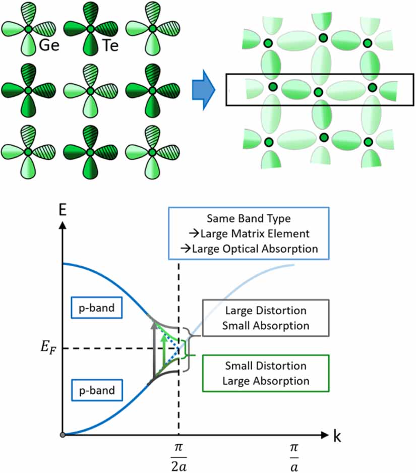
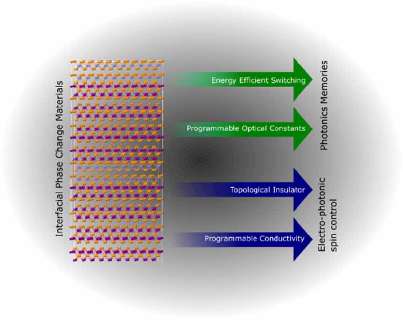
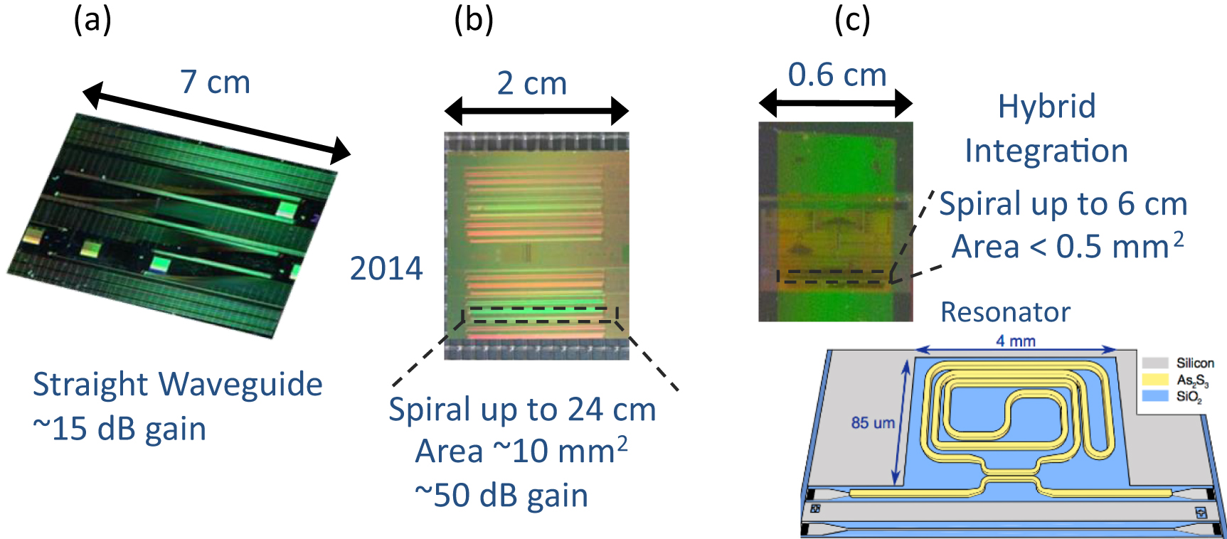
Figure 17. Schematic illustration of possible use of a-Se in a single-line detector with strip electrodes. The field is horizontal (along x) and radiation absorption is vertical (along y).
Download figure:
Standard image High-resolution image
Concluding remarks
Today doped and alloyed a-Se alloys find a rich niche in x-ray imaging detector applications based on direct (already commercialized) and indirect conversion (prototype). We outlined a-Se's distinct advantages over its competitors, then formulated the current and potential problems, and the road ahead. While ideally suited for mammography, there are challenges to use a-Se at higher x-ray energies and also in single-photon detectors where energy dispersion is highly desirable. Both advances in science and technology are needed to further enhance the performance of present detectors (such as increased resolution, greater quality control etc) but also in the development of imaging detectors at higher x-ray energies with new functionalities e.g. dual energy imaging, whose recent integration with CMOS imagers for high-resolution imaging is expected to grow significantly in the near future.
Acknowledgments
The authors are most grateful to John Rowlands for mentoring the present authors through many years on the science and technology of flat panel direct conversion detectors. The authors thank NSERC for financial support through their discovery grants program.
Data availability statement
No new data were created or analyzed in this study.